 Facebook
 Google
 GitHub
 Linkedin
Designing I/O Drivers for Integrated Circuit I2C Modules
This article discusses designing input/output drivers for integrated circuit I2C modules.
I²C is a synchronous, multi-master, multi-slave serial interface that allows microchips to communicate with one another. As an open-drain/open-collector communication standard, I²C allows integrated circuits (ICs) to communicate even when they use different voltage rails.
The Four Speeds of the I²C Standard
There are four speeds of operation in the I²C standard:
- Standard mode: 100 kHz
- Fast mode: 400 kHz
- Fast mode plus: 1 MHz
- High-speed mode: 3.4 MHz
I²C Bus Lines: Serial Data and Serial Clock
The I²C bus uses two lines—serial data (SDA) and serial clock (SCL)—and all I²C master and slave devices are connected by only these two lines. Each device can be both a transmitter and a receiver.
Both the SDA and SCL signals are bidirectional. The SDA and SCL pins of each device are open-drain pins. They have pull-up resistors connected to them to obtain logic 1. Logic 1 depends on the supply voltage; there is no standard bus voltage.
The I²C Cell Structure
Let us discuss the I²C I/O cell structure integrated in the ICs. The block diagram of the I²C I/O cell structure is shown in Figure 1.
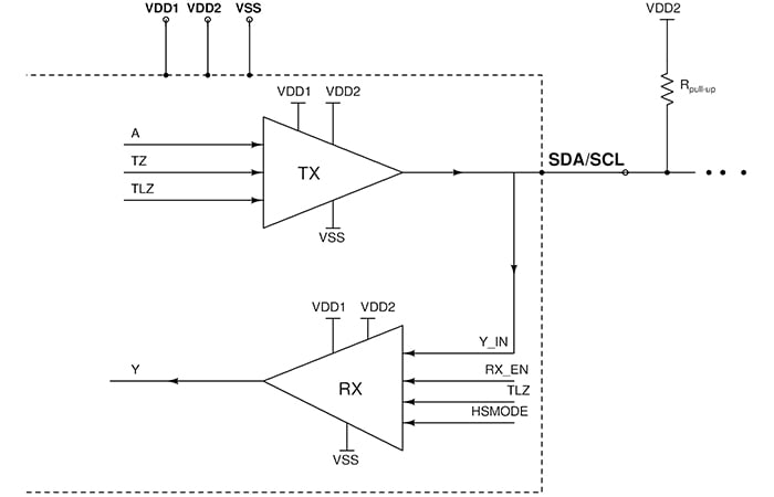
Figure 1. Block diagram of I²C I/O driver
The TX block is enabled in the transmission time frame while the RX block is enabled in the reception time frame.
VDD1 and VDD2 are two different voltage rails where the master and slave operate. VDD1 is the chip’s supply for internal operations and VDD2 is the supply voltage the external system uses. To support different voltage rails, a level shifter is required to translate signals from one supply voltage to another.
Transmitter Circuit in I²C Modules
The transmitter circuit block diagram is shown in Figure 2.

Figure 2. Transmitter block diagram
A is the data signal to be transmitted out on the pin SDA/SCL. TLZ is the tristate control during a VDD1 power-down. TZ is level shifted from VDD1 to VDD2 to enable the output open-drain buffer for A_OUT.
If VDD1 is powered down during the operation of the system intentionally or unintentionally with VDD2 still active, the TZ enable signal goes low or is mostly undetermined. This may enable the output buffer to A_OUT.
The TLZ signal is used as a fail-safe mechanism. The TLZ is pulled down during the power down, which pulls the TZ signal high. At this point, the output buffer is not enabled anymore. The open drain buffer would be in a tristate condition when VDD1 is powered down.
To learn more about the use cases, benefits, and applications of using an I²C buffer, check out AAC's technical article on when to use an I²C buffer.
Receiver Circuit in I²C Modules
The receiver circuit block diagram is shown in Figure 3.
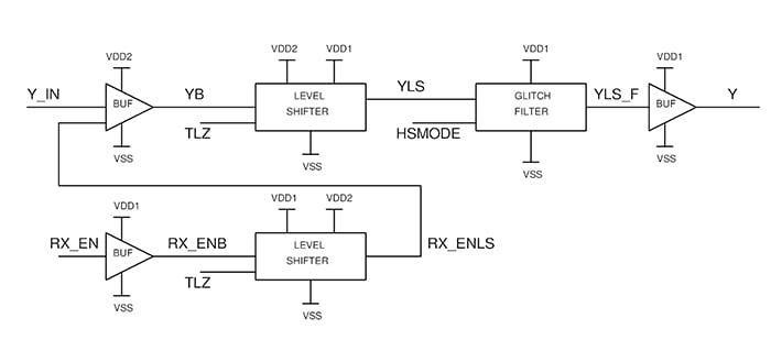
Figure 3. Receiver block diagram
The receiver circuit is enabled with an RX_EN signal. TLZ has the same functionality as that in the transmitter block. The HSMODE signal enables the high-speed mode.
The RX_EN signal is level shifted from VDD1 to VDD2 to enable the buffer that receives the Y_IN signal. A level shifter then shifts the buffered Y_IN signal to the VDD1 voltage rail.
Using a Glitch Filter
I²C signals are prone to noise and disturbances. As a result, you need a glitch filter to filter out all the unwanted glitches and allow only valid signals to pass. In the standard/fast mode, glitches of <= 50ns are suppressed. In high-speed mode, glitches of <= 10ns are suppressed.
The glitch filter design is shown in Figure 4 and the timing diagram is shown in Figure 5.
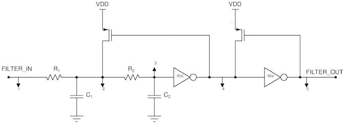
Figure 4. Glitch filter design
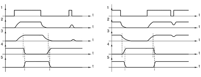
Figure 5. Timing diagram of glitch filter
The RC time constant delays passing signals and suppresses any glitches. The R1, C1, R2, C2 combination determines the pulse width of glitches to be suppressed. In accordance with I²C specifications, the receiver should be capable of suppressing glitch pulses of <= 50ns in standard and fast modes and <= 10ns in high-speed mode.
The output signal from the glitch filter is buffered and is processed for further operations by the IC.
Pull-Up Resistors in an Open-Drain Configuration
The output buffer on I²C lines are in open-drain configuration, which we discuss in further detail in our article on the hardware needed for an I²C bus. Any I²C device can only drive low on these I²C lines or tristate them. To obtain a logic high, the pull-up resistors are required to pull them to the voltage rail during a tristate condition.
When the device is driving low, these pull-up resistors draw current via the NMOS as shown in Figure 6.
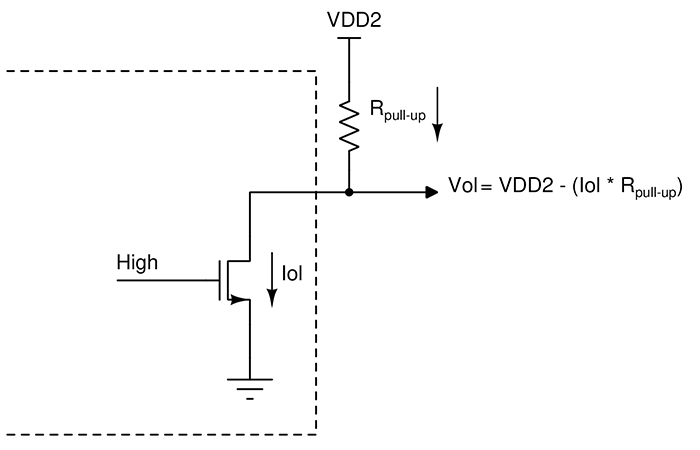
Figure 6. Open-drain configuration
The rise time depends on the pull-up resistor and parasitic capacitance time constant and is usually longer than the fall time because the fall is driven by the device (i.e. by the NMOS). Hence, different pull-up resistors are required for different speeds of operation.
For more information about pull-up resistors and capacitive loads, please check out our article on I²C mathematics for capacitance and resistance.
Learn More About the I²C Bus
- I2C Bus Firmware Implementation Details
- Reading The-I2C-Bus on an Oscilloscope
- Implementing I2C with an EFM8 Microcontroller
- Program a PIC Microcontroller as an I2C Slave Device for Custom Sensor and I/O Interfacing


How is this glitch filter in figure 4 supposed to work? Having the input signal over an input resistor working against VDD will not be able to drive any level to the input of the first inverter…