 Facebook
 Google
 GitHub
 Linkedin
I2C Design Mathematics: Capacitance and Resistance
This article looks at the mathematical calculations used to size the pull-up resistors and determine the maximum length of circuit traces.
Learn about I2C and some of the design challenges that comes with it, including logic thresholds, factors that affect capacitance, and minimum and maximum pull-up resistance.
This article covers what variables affect the capacitance of your bus. It also looks at the mathematical calculations used to size the pull-up resistors and determine the maximum length of circuit traces. Let's start by discussing what I2C actually is.
Related Information
- Introduction to the I2C Bus
- I2C Bus Hardware Implementation Details
- I2C Bus Firmware Implementation Details
- Reading The-I2C-Bus on an Oscilloscope
About I2C
I²C is a multi-master, multi-slave serial interface that allows microchips to communicate with one another at standard speeds of 100 kHz (Standard Mode), 400 kHz (Fast Mode), 1 MHz (Fast Mode Plus), and 3.4 MHz (High-Speed Mode).
One of our previous articles, I²C Bus Hardware Implementation Details, explains the mechanism in great detail. The bus specification can be found on NXP's website.
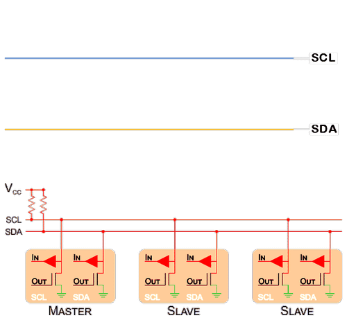
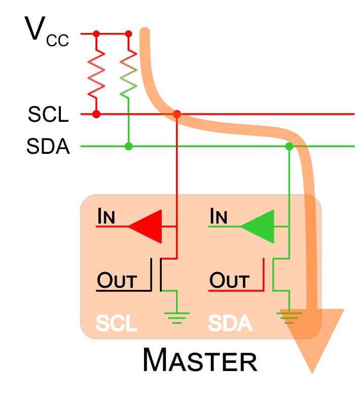
Shown above is an I²C hardware configuration along with simplified clock and data waveforms.
Real-life I²C transactions are not the square-wave pulses commonly depicted in drawings. The circuits have an inherent impedance due to the presence of parasitic capacitance and the use of pull-up resistors.
Logic-high to logic-low transitions involve current discharging through the low-impedance channel of an NMOS transistor—these transitions are rapid. The logic-low to logic-high transitions, however, involve current that must flow through a relatively high-value pull-up resistor. Lower pull-up resistance leads to faster transitions but also to higher current consumption (when the signal is logic low); higher pull-up resistance leads to slower transitions and reduced current consumption. The value of the resistor chosen becomes increasingly important at higher frequencies.
Positive transitions appear rounded due to the pull-up resistors in the logic-low-to-logic-high current path.
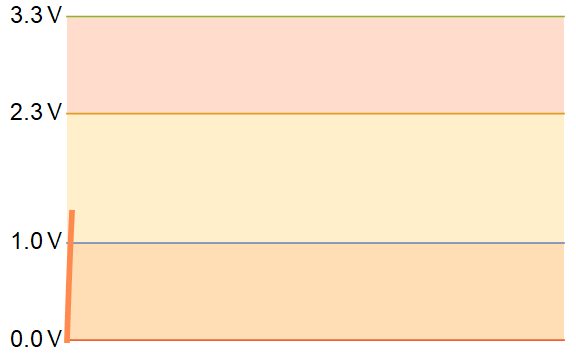
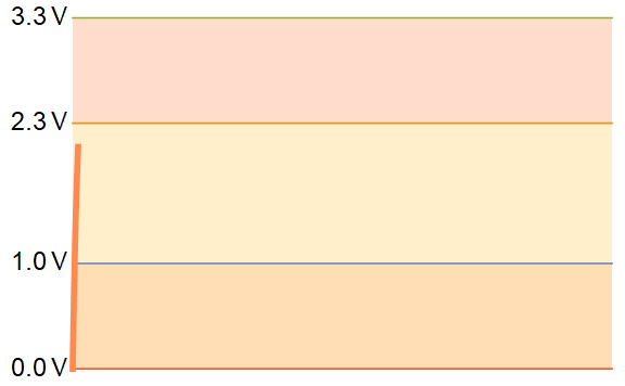
Any increase in bus capacitance or resistance will increase the logic-high transition time. At a certain point, the potential difference will not even reach the logic-high threshold, or it will not remain there long enough before transitioning back to logic low.
In the above graph, the RC time constant is too large and the logic-high threshold is not reached.
Different I²C devices can have different logic thresholds. The preceding graphs all assume transitions with $$V_{LL}=0.3*3.3 V = 1 V$$ and $$V_{LH}=0.7*3.3 V=2.3 V$$, but this is not always the case. The ADP5062, for example, has transitions at $$V_{LL}=0.5 V$$ and $$V_{LH}=1.2 V$$.
Chips with different threshold voltages can be used on the same bus; when this is the case, calculations should be made using the highest logic-high threshold voltage and lowest logic-low threshold voltage.
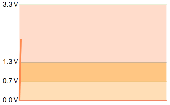
This graph shows a hypothetical logic-low threshold voltage of 0.7 V and a hypothetical logic-high threshold voltage of 1.3 V. These low values increase the time spent in the logic-high state without significantly altering the time spent in the logic-low state. This configuration allows for higher-frequency operation.
Capacitance
The NXP specification states that the maximum overall bus capacitance is 400 pF for Standard Mode and Fast Mode devices and 550 pF for Fast Mode Plus devices. You should not add capacitors to the I²C lines in order to reach these upper capacitance limits—a lower bus capacitance is better.
Dielectrics
Your circuit board base material can affect the overall capacitance of your bus. The dielectric constant for most PCB base materials is in the range of 2.5≲ε≲5 (ε is frequency dependent).
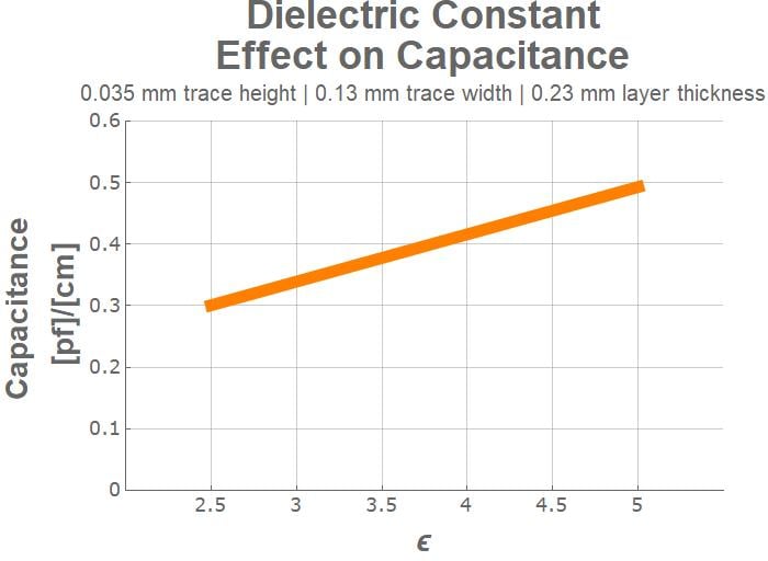
This graph shows the effect of dielectric constant on the capacitance of a microstrip line.
The more expensive base materials tend to have lower overall permittivity—which decreases the overall capacitance of your traces, which is the goal. It’s possible to decrease overall trace capacitance by 45% by choosing TLT (ε=2.5) instead of Policlad 370HR (εFR4=4.5).
Sources of Increased Bus Capacitance
Sources of bus capacitance include the ICs on the bus, microstrip traces, and nearby signal traces and power planes. Also, capacitive fringe effects cannot be ignored in the case of small circuit boards or when I²C traces are near the edge of the board.
Any metal or dielectric near the I²C lines can increase your overall capacitance, but in many cases the effect is negligible.
Insignificant Sources of Capacitance
Parasitic bond and package capacitance is not something that you can control. Fortunately, it’s only approximately 1-2 pF per signal line (see this document for more information). In other words, it’s not going to be a significant consideration in your overall circuit. This 1-2 pF capacitance is included in the estimate in the following paragraph.
Significant Sources of Capacitance
ICs Used in the Circuit
The NXP specification lists a “maximum capacitance for each I/O pin” of 10 pF. Each IC that you add will increase the overall bus capacitance by approximately 10 pF (see the datasheet for the specific IC), and then you must also consider the capacitance associated with the traces that connect the IC to the bus.
Copper Trace Capacitance
When we say "copper trace capacitance" here, we're referring to single trace over dielectric over ground. The capacitive coupling between the I2C signal lines and the ground plane can be significant if the ICs are far from each other, or multiple ICs are on the I2C bus. For long runs, separate the I2C lines from one another by several trace widths (or place the Vdd and ground traces between the signal traces) to reduce capacitive coupling effects between the two signal lines.
To calculate the capacitive coupling between a signal and a ground plane (or a power plane), use the following equation, which takes into account fringe effects.
$$C[pf] \approx \frac{0.264\tfrac{[pf]}{[mm]}(\epsilon_r+1.41)}{Ln\left(\frac{0.598\tfrac{1}{[mm]}\cdot \text{layer height}} {0.08\tfrac{1}{[mm]} \cdot \text{trace width}+0.1\tfrac{1}{[mm]}\cdot \text{trace thickness}}\right)}$$
Modified from "High Speed Digital Design" by Johnson and Graham
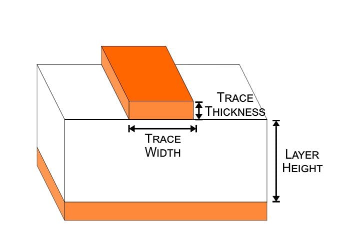
The calculation below is an example calculation for adjacent layers of a four-layer stack with the following realistic parameters: εFR4 = 4.5, trace width = 0.13 mm, layer height = 0.23 mm, trace thickness = 0.035 mm.
$$C[pf] \approx \frac{0.264\tfrac{[pf]}{[cm]}(4.5+1.41)}{Ln\left(\frac{0.598\tfrac{1}{[mm]}\cdot 0.23\text{[mm]}} {0.08\tfrac{1}{[mm]} \cdot 0.13\text{[mm]}+0.1\tfrac{1}{[mm]}\cdot 0.035\text{[mm]}}\right)}=0.68\tfrac{pF}{cm}$$
Effect of Apertures on Microstrip Capacitance
It is possible to decrease the capacitance by increasing the distance to the ground plane—this is accomplished by placing the signal traces on layers that are one or more layers removed from the ground plane. It is also possible to remove copper from a plane layer so as to create a copper void underneath the trace. This void is referred to as an aperture.
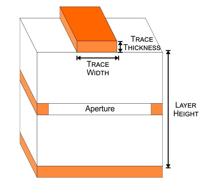
So what effect does this have on the overall capacitance? If we use the same parameters as in the previous calculation but then add 0.965 mm between the signal trace and the ground plane, we achieve a ~40% reduction in capacitance. If your PCB layout allows for a suitably large aperture directly beneath the signal trace, this might be a worthwhile improvement in designs with very long traces.
$$C[pf] \approx \frac{0.264\tfrac{[pf]}{[cm]}(4.5+1.41)}{Ln\left(\frac{0.598\tfrac{1}{[mm]}\left (0.23\text{[mm]}+0.035 \text{[mm]}+0.93\text{[mm]}\right )} {0.08\tfrac{1}{[mm]} \cdot 0.13\text{[mm]}+0.1\tfrac{1}{[mm]}\cdot 0.035\text{[mm]}}\right)}=0.40\tfrac{pF}{cm}$$
Resistors
Two requirements govern the minimum pull-up resistance. First, the pull-up resistor must limit the current to a level that does not exceed the maximum drain current of the output transistor. Second, the resistor must prevent excessive current consumption when the SCL or SDA signal is in the logic-low state. In practice, current consumption is the dominant consideration because typically there is no need to use a resistance that is small enough to endanger the output transistor.
As an example, let’s say that we have a 3.3 V bus and want to limit the current to 3 mA.
$$R_{min}=\frac{V_{\text{bus}}}{I_{\text{Max}}}=\frac{3.3\text[V]}{3\text{[ma]}}=1.1k\Omega$$
If we assume that the clock and data lines both have a 50% duty cycle, the power consumption is
$$P=0.5\cdot2\cdot\frac{V^2}{R}=\frac{(3.3 [V])^2}{1100\Omega}\approx 10\text[mW]$$
Low-valued pull-up resistors produce faster transitions and a “sharper” wave, but they also lead to higher power dissipation.
Calculating the Maximum Value of Pull-Up Resistors
To ensure proper functionality, the designer must ensure that an I2C device’s timing requirements are satisfied.
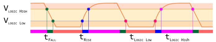
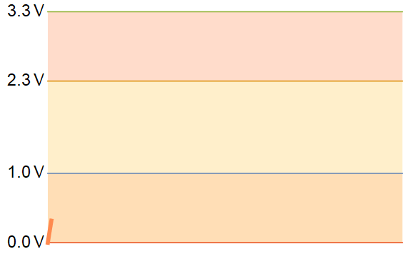
The above graph illustrates the segments of an I2C transaction that correspond to rise time, fall time, time spent in logic-low state, and time spent in logic-high state. Appropriate values for these timing parameters are typically indicated in a device’s datasheet. The graph is not to scale.
High-value pull-up resistors will increase the transition time to the logic-high threshold, which might prevent the IC from functioning correctly.
The logic-high rise time is too great, and the logic-high threshold has not been met. Consequently, devices on this bus will not be able to communicate.
Calculating the maximum value of a pull-up resistor requires knowing the rise-time requirement. Then, exponential functions are used to model the curve and find the time required to reach the logic-high threshold voltage after passing the logic-low threshold voltage.
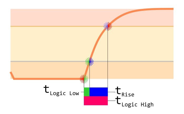
The rising curve is given by the exponential function shown below. To solve for rise time, subtract the time required to reach the logic-high threshold from the time to reach the logic-low threshold. The equation provides the vertical axis (voltage) as it relates to the horizontal axis (time). It is necessary to rearrange the equation to solve for time before determining the difference in time.
$$V_{\text{Logic High}}=V_{\text{cc}}\left (1−e^{\left ( \frac{−t_{\text{Logic High}}}{R_{\text{Pull Up}}\cdot C_{\text{Bus}}}\right )} \right )$$
$$t_{\text{Logic High}}=C_{\text{Bus}}\cdot R_{\text{Pull Up}}\cdot Ln\left ( \frac{V_{\text{CC}}}{V_{\text{CC}}−V_{\text{Logic High}}}\right )$$
The initial equation arranged to solve for the time to reach the logic-high threshold voltage
$$V_{\text{Logic Low}}=V_{\text{cc}}\left (1−e^{\left ( \frac{−t_{\text{Logic Low}}}{R_{\text{Pull Up}}\cdot C_{\text{Bus}}}\right )} \right )$$
$$t_{\text{Logic Low}}=C_{\text{Bus}}\cdot R_{\text{Pull Up}}\cdot Ln\left ( \frac{V_{\text{CC}}}{V_{\text{CC}}−V_{\text{Logic Low}}}\right )$$
The initial equation arranged to solve for the time to reach the logic-low threshold voltage
Rearrange to solve for $$R_{\text{Pull Up}}$$ and it becomes
$$R_{\text{Pull Up Max}}=\frac{t_{\text{Rise Time}}}{Ln\left ( \frac{V_{\text{cc}}−V_{\text{Logic Low}}}{V_{\text{cc}}−V_{\text{Logic High}}} \right )\cdot C_{\text{bus}}}$$
This is the final form to use in calculations for the maximum pull-up resistance; tRise Time, VLogic Low, and VLogic High are given in the datasheet, and CBus is estimated based on the characteristics of your circuit. Choosing the arbitrary values of tRise Time = 150 ns, VLogic Low = 0.5 V, and VLogic High = 1.2 V, and assuming a bus capacitance of 150 pF, we have the following:
$$R_{\text{Pull Up Max}}=\frac{1.5\cdot10^{-9}[s]}{Ln \left ( \frac{3.3 [V]-0.5[V]}{3.3 [V]-1.2 [V]}\right )}\approx 3500\Omega$$
Summary
The value of an I²C pull-up resistor must be large enough to reduce unnecessary current consumption and small enough to produce an acceptable rise time. The calculations presented in this article can help you to find a suitable value, but if you really want to optimize your I²C bus, you will probably need to measure the signals with an oscilloscope (use a low-capacitance probe if possible) and adjust the pull-up resistance until you achieve the desired timing characteristics.
Related Content


Amazing article ! I have a question relative to capacitance for microstrips. Do we have to take in consideration a potential ground plane surrounding the trace for the calculation ? If yes, what kind of clearance do we need to have between the signal trace and the ground plane in order to keep the capacitance as low as possible ?
Don’t you think the INPUT and OUTPUT need to be reversed in the following images
https://www.allaboutcircuits.com/uploads/articles/Hughes_Technical_I2CMathematics_schematicpairing.gif
https://www.allaboutcircuits.com/uploads/articles/Hughes_TechnicalArticle_I2C_SinkCurrent.jpg
If they are correct, I think, there may be a descrepancy in this page and the following page
https://www.allaboutcircuits.com/technical-articles/the-i2c-bus-hardware-implementation-details
Kindly explain !
What about combine current leakage in the bus which can limit the maximal value of pull-up resistance? Important for slow and long low power I2C bus.
Thanks for good article