 Facebook
 Google
 GitHub
 Linkedin
The I2C Bus: Firmware Implementation Details
Understand the I2C protocol in the context of firmware design and make your projects seamless.
Master the I2C protocol.
Supporting Information
- Introduction to the I2C Bus
- The I2C Bus: Hardware Implementation Details
- The I2C Bus: When to Use an I2C Buffer
The Typical Transaction
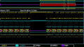
Devices communicating via I2C must conform to a specific sequence of events. Each event corresponds to a certain way of controlling the clock (SCL) and data (SDA) lines; as discussed in the “Supporting Information” articles listed above, these two signals are the only means by which devices on the bus can share information. We will refer to one communication sequence as a “transaction”; this word is more appropriate than “transmission” because every transaction involves both transmitted data and received data, though in some cases the only received data is an acknowledge (ACK) or not-acknowledge (NACK) bit detected by the master. The following timing diagram shows a typical I2C transaction.

Note the following:
- The dotted line corresponding to the logic-high portion of the clock reminds us that logic high (for both SCL and SDA) is the “recessive” state—in other words, the signal naturally floats up to logic high via the pull-up resistor. The “dominant” state is logic low, because the signal will be low only when a device is actually driving it low.
- The transaction begins with a “start bit.” Every I2C transaction must begin with a start bit, which is defined as a falling edge on SDA while SCL is logic high.
- The transaction ends with a “stop bit,” defined as a rising edge on SDA while SCL is logic high. I2C transactions must end with a stop bit; however, as discussed later in the article, multiple start bits can occur before a stop bit is generated.
- Data is valid while the clock is high and changes state while the clock is low; digital communication systems are usually edge-driven, so in practice the data is read on the rising edge of the clock and updated on the falling edge of the clock.
- Information is exchanged one-byte-at-a-time, starting with the most significant bit, and each byte is followed by an ACK or NACK.
- You might expect ACK to be indicated by logic high and NACK to be indicated by logic low, but this is not the case. ACK is logic low and NACK is logic high. This is necessary because high is the recessive state—if the slave is nonfunctional, the signal naturally floats up to a NACK. Likewise, ACK (indicated by the dominant logic low) can be transmitted only if the device is operational and ready to continue with the transaction.
The following list describes the sequence of events in the above transaction:
- The master generates a start bit to initiate the transaction.
- The master transmits the 7-bit address corresponding to the slave with which it wants to communicate.
- The final bit in the first one-byte segment is the read/write indicator. The master sets this bit to logic high if it wants to read data from the slave, or to logic low if it wants to write data to the slave.
- The next byte is the first data byte. This comes from either the master or the slave, depending on the state of the read/write bit. As usual, we have 8 bits of data, starting with the most significant bit.
- The data byte is followed by an ACK or a NACK, generated by the master if this is a read transaction or by the slave if this is a write transaction. ACK and NACK can mean different things depending on the firmware or low-level-hardware design of the communicating devices. For example, the master could use NACK to say “this is the last data byte,” or if the slave knows how much data to send, it could use ACK to confirm that the data was successfully received.
- The transaction is terminated with a stop bit generated by the master.
How Many Bytes?
Every transaction begins the same way: start bit, address, read/write, ACK/NACK. After that, any number of bytes can be sent from master to slave or from slave to master, with each byte followed by ACK or NACK. NACK can be useful as a way to say “stop sending data!” For example, the master might want to receive a continuous stream of data from a slave device (such as a temperature sensor); each byte would be followed by ACK, and if the master needs to turn its attention to something else, it can NACK the slave and begin a new transaction whenever it is ready.

Start without a Stop
The I2C protocol allows for something called a “repeated start” condition. This occurs when the master initiates a transaction with a start bit then initiates a new transaction via another start bit without an intervening stop bit, as follows:

This feature can be used whenever a single master needs to perform two or more separate transactions. However, there is a situation in which the repeated start condition is particularly handy:
Let’s say you have a slave device that stores information in a bank of registers. You want to retrieve data from register address 160, 0xA0 in hex. The I2C protocol does not allow the master to send data and receive data in a single transaction. Consequently, you have to perform a write transaction to specify the register address and then a separate read transaction to retrieve the data. This approach can lead to problems, though, because the master releases the bus at the end of the first transaction, and thus another master could claim the bus and prevent the first master from getting the data it needs. Furthermore, the second master might communicate with the same slave and specify a different register address . . . if the first master then claims the bus and reads data without re-specifying the register address, it will read the wrong data! If the second master then tries to perform the read transaction in its write-then-read procedure, it also will end up with the wrong data! This is a system failure waiting to happen—fortunately, the repeated start condition can prevent this mess by initiating the second (read) transaction without releasing the bus:

When Masters Can’t Get Along
Part of what makes I2C so versatile is its support for multiple masters. But as the previous section demonstrates, masters don’t always play well together. A device’s I2C logic must be able to determine if the bus is free; if another master has claimed the bus, the device waits until the current transaction concludes before initiating its own transaction. But what happens when two (or more) masters attempt to initiate a transaction at the same time? I2C provides an effective and surprisingly simple solution to this otherwise irksome problem. The process is referred to as “arbitration,” and it relies upon the flexibility of I2C’s open-drain bus configuration: if one master attempts to drive the signal logic high and the other attempts logic low, the logic-low master will “win,” and furthermore, the “loser” can detect that the actual output state is not the intended output state:

This diagram conveys the basis of I2C arbitration; the process occurs as follows:
- Both masters generate a start bit and proceed with their transmissions.
- If the masters happen to choose the same logic levels, nothing happens.
- As soon as the masters attempt to impose different logic levels, the master driving the signal low is proclaimed the winner; the loser detects the logic mismatch and abandons its transmission.
Take a moment to appreciate the simplicity and efficacy of this arrangement:
- The winner continues its transmission without interruption—no corrupted data, no driver contention, no need to restart the transaction.
- Theoretically the loser could monitor the slave address during the arbitration process and actually make a proper response if it happens to be the addressed slave.
- If the competing masters are both requesting data from the same slave, the arbitration process does not unnecessarily interrupt either transaction—no mismatch will be detected, and the slave will output its data to the bus such that multiple masters can receive it.
Conclusion
This article has covered the prominent I2C details that influence the design of firmware or low-level hardware. If your microcontroller includes dedicated I2C or SMBus hardware, some of the implementation details will be handled automatically. This is convenient but certainly not an excuse for ignorance because you will still need to know at least a little bit (probably more than a little bit) about how I2C really works. Furthermore, if you ever find yourself stranded on a desert island without an I2C peripheral, the information presented here will put you well on your way to designing a firmware-only (aka “bit-banging”) I2C routine.
Related Content


What does this article have to do with firmware implementation details?