Facebook
 Google
 GitHub
 Linkedin
Offset Error and Gain Error in a Bipolar ADC and Differential ADC
Concerning analog-to-digital converters (ADCs), learn about offset errors and gain errors in a bipolar ADC and differential ADC as well as offset error single-point calibration.
In a previous article, we discussed how the offset error could affect the transfer function of a unipolar ADC. With that in mind, the inputs of a unipolar ADC can only accept positive voltages. In contrast, the inputs of a bipolar ADC can process both positive and negative voltages. In this article, we’ll explore the offset and gain error specifications in bipolar and differential ADCs; and learn about the single-point calibration of the offset error.
Transfer Functions—Bipolar ADC Ideal Characteristic Curves
The transfer function of an ideal three-bit ADC with the offset binary output coding scheme is shown in Figure 1.
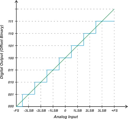
Figure 1. The transfer function of an ideal three-bit ADC with offset binary output coding,
As a refresher, with the offset binary system, the center of the mid-scale code (100 in our example) corresponds to the 0 V input. Codes below 100 represent a negative input voltage and digital values above 100 correspond to a positive analog input. However, note that the sequence of the codes on the vertical axis is exactly the same as that of a unipolar ADC. The straight line that goes through the midpoint of the steps provides us with a linear model of the ADC staircase response.
Another thing to be aware of is that the above characteristic curve can represent a unipolar ADC with differential inputs as well. Since the output codes below 100 represent a negative value, it is helpful to plot the above transfer function as shown in Figure 2.
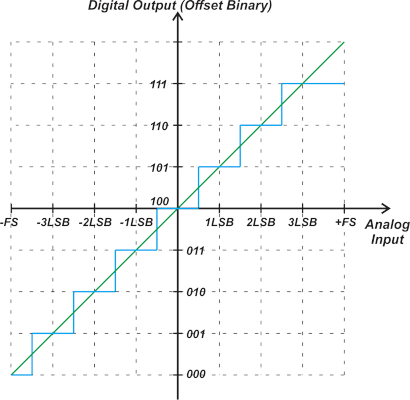
Figure 2. Transfer function showing the output codes below 100.
Bipolar ADC Offset Error
For an ADC with the offset binary coding scheme, the offset error can be found by comparing the actual midscale transition from 100…00 to 100…01 with the corresponding transition in an ideal ADC. As shown in Figure 2, this transition should ideally occur at +0.5 LSB. Figure 3 shows a three-bit bipolar ADC with an offset value of -1 LSB.
Note that the midscale transition from 100 to 101 occurs at +1.5 LSB rather than +0.5 LSB.
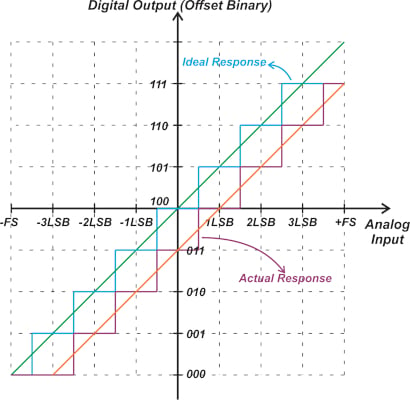
Figure 3. The transfer function of a three-bit bipolar ADC with an offset value of -1 LSB.
A three-bit bipolar ADC with a positive offset is shown in Figure 4.
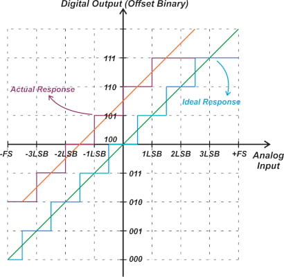
Figure 4. A three-bit bipolar ADC with a positive offset.
In this case, the first transition for a positive input occurs at +1 LSB from 110 to 111. For an ideal ADC, this transition should occur at +2.5 LSB. As such, the actual transfer function has an offset of +1.5 LSB. You can also get the same result by examining the linear model of the actual transfer curve which is shown by the orange straight line in Figure 4.
Bipolar ADC Gain Error
Similar to a unipolar ADC, the gain error for a bipolar ADC can be defined as the deviation of the actual last transition from the ideal last transition after the offset error is trimmed out. The gain error can also be defined as the deviation of the slope of the actual linear model from the slope of the ideal straight line model.
As an example, consider the characteristic curve shown in Figure 5.
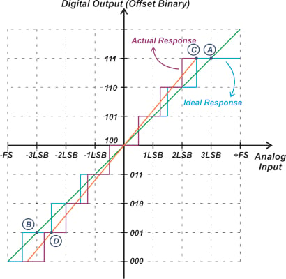
Figure 5. Characteristic curve example
In this example, points A and C are 0.5 LSB above the last transition of the ideal and actual response, respectively. Similarly, points B and D are chosen close to the negative full-scale (0.5 LSB below the 010 to 001 transition) on the ideal and actual transfer curves, respectively. The line going through A and B is the ideal response, whereas the line going through C and D is the actual response of the system. The actual slope can be compared with the ideal slope to determine the gain error.
In the above example, the ideal slope is given by:
\[Slope_{\,i}=\frac{Code_{A}-Code_{B}}{V_{in,A}-V_{in,B}} = \frac{3-(-3)}{3LSB-(-3LSB)}=1\frac{Count}{LSB}\]
In this equation, the decimal equivalent of the output codes is used. Also, pay attention to the sign of the codes. As expected the ideal slope is one. The measured slope can be found in a similar manner:
\[Slope_{\,m}=\frac{Code_{\,C}-Code_{\,D}}{V_{in,C}-V_{in,D}}=\frac{3-(-3)}{2.5LSB-(-2.5LSB)}=\frac{6}{5}\frac{Count}{LSB}\]
The gain error can be defined by the following equation:
\[Gain\,Error=\frac{Slope_{\,m}-Slope_{\,i}}{Slope_{\,i}}=\frac{\frac{6}{5}-1}{1}=0.2\]
This means that the measured response has a 20% gain error. With high-performance ADCs, the gain error might be small enough to be expressed in ppm.
Keep in mind that in practice, the points we choose to find the slope of the response are not necessarily the endpoints of the transfer function. Depending on the test signals available in the system and the input range over which the system is linear, we can choose appropriate points to determine the slope of the transfer function. For example, an accurate 1.5 V input that is already available in the system might be considered close enough to the positive full-scale value when determining the slope of an ADC that has a full-scale value of 3 V.
Offset and Gain Error Leads to Unused Input and Output Values
With both unipolar and bipolar ADCs, the offset error leads to unused input range and unused output codes. Figure 6 shows how a negative offset restricts the lower limit of the input range to values higher than -FS. With a negative offset, a range of the output codes below the nominal maximum code might not be used as well.
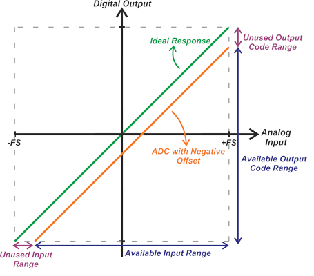
Figure 6. A graph showing how a negative offset restricts the input range's lower limit to values higher than -FS.
As you can probably imagine, the offset error will affect the range of a unipolar ADC in a similar manner. As an example, consider a unipolar 12-bit ADC with a 2.5 V full-scale voltage that has an offset of -8 mV. This corresponds to an offset of about -13 LSB. The ideal straight-line response is shifted downward by 13 LSB. Therefore, as shown in Figure 7, the input analog range is reduced by 13 LSB (or 8 mV), and the last 13 output codes are not used.
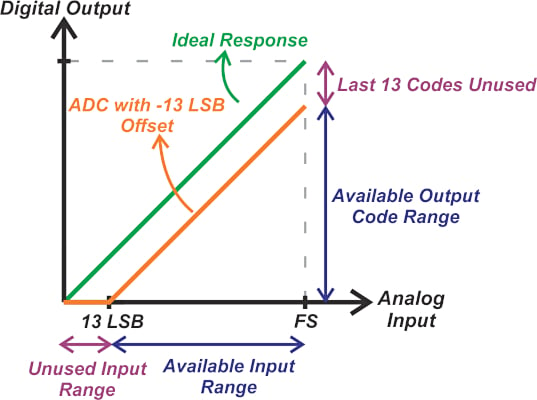
Figure 7. A graph showing the reduction of input analog range by 13 LSB.
It's important to remember that the same offset voltage in a higher resolution ADC can lead to a larger unused code range. For example, the same -8 mV of offset in a 16-bit ADC with FS = 2.5 V corresponds to about -210 LSBs. In this case, the last 210 output codes are not used. Figure 8 shows the effect of a positive offset on the ADC input and output range.
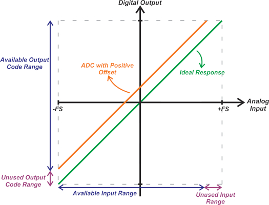
Figure 8. The effect of a positive offset on the ADC's input and output range.
In this case, a number of codes from the lower end of the output code range are not used and the maximum ADC output is reached at an input level smaller than +FS. A positive gain error can limit the input range from both ends, as illustrated in Figure 9.
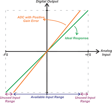
Figure 9. A graph showing how a positive gain error can limit the input range at both ends.
Similarly, a negative gain error can lead to unused output codes at both ends of the nominal range (Figure 10).
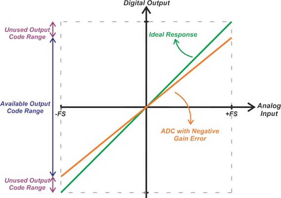
Figure 10. How a negative gain error can lead to unused output codes at both ends of the nominal range.
Now that we’re familiar with the offset and gain error concepts in ADCs, we can delve into a discussion on the calibration of these two error terms.
ADC Gain and Offset Calibration
The offset and gain errors can be easily calibrated out in the digital domain. To do this, accurate analog inputs should be applied to the ADC to determine the actual response. With the actual response known, the ADC output code can be corrected in the digital domain to match that of the ideal response.
Since a given ADC code doesn’t correspond to a single analog input value, the actual ADC response can be determined only by measuring the code transitions. This requires a precision source that can generate different voltage levels. Figure 11 shows a test setup that can be used to determine the code transitions.
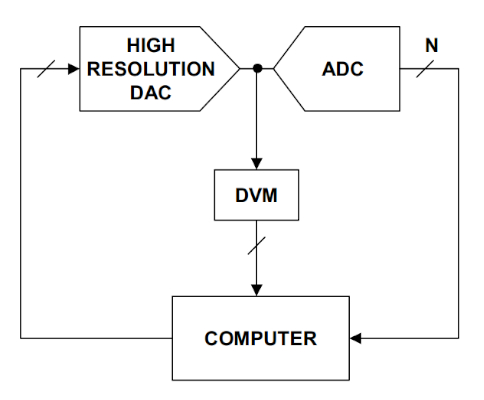
Figure 11. An example test setup to determine code transitions Image used courtesy of Analog Devices.
In this case, a high-resolution digital-to-analog converter (DAC) is used to generate different voltage levels at the ADC input. The DAC should provide an accuracy significantly greater than the ADC under test. In addition, the voltmeter at the DAC output provides an accurate measurement of the voltage level at which a code transition occurs. The output of the voltmeter and the ADC are processed to determine the offset and gain errors, as well as the nonlinearity of the ADC. This PC-based method can use digital signal processing (DSP) techniques, such as signal averaging, to reduce the effect of the ADC noise on the measurements.
In many applications, such as sensor measurement systems, it is not possible to use the above setup to measure the code transitions. In these cases, we might have only one or two precision voltage levels available in the system, enabling a single-point or two-point measurement. These tests can only approximate the actual response and cannot completely eliminate the offset and gain errors. However, they are still effective methods that can significantly reduce the offset and gain errors.
Offset Calibration—Single-point Calibration
A single-point calibration measures the ADC response at a single point on the transfer function and uses the result to reduce the offset error. The ground potential is an accurate, commonly-used test input for single-point calibration as it is already available in the system. As an example of applying this method, consider the response is shown in Figure 3, which is repeated below for convenience as Figure 12.
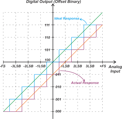
Figure 12. A repeat of Figure 3 shows the transfer function of a three-bit bipolar ADC with an offset value of -1 LSB.
If we apply zero volts to this ADC, the output is 011. Comparing this with the ideal value, 100, we can determine that the ADC has an offset of -1 LSB. Another example is shown below in Figure 13.
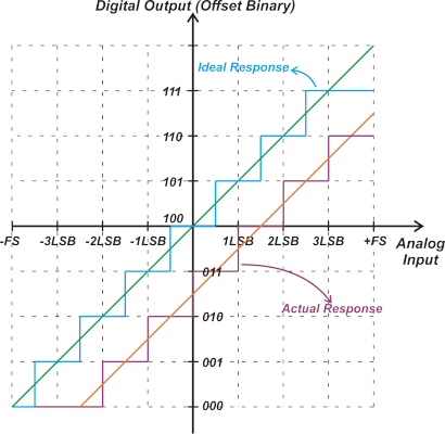
Figure 13. An example showing the ADC offset of -1 LSB after applying zero volts to the ADC.
In this case, the transition from 010 to 011 occurs just below zero volts. Again shorting the input to the ground produces 011. Based on this single-point measurement, the ADC offset is -1 LSB. However, considering the code transitions, we observe that the actual offset is -1.5 LSB. As you can see, with a single-point measurement, the error in determining the offset can be as large as ±0.5 LSB. Despite that, this error can be acceptable in most applications, especially considering the fact that this method has the minimum cost and complexity. A single-point measurement cannot determine the gain error.
Once the offset is determined, we can compensate for it by subtracting the offset from every ADC reading. A single-point calibration through the ground potential can be used only with bipolar or differential input ADCs. With a unipolar ADC, a negative offset leads to unused input values on the lower end of the nominal input range. The example depicted below (Figure 14) further clarifies this issue.
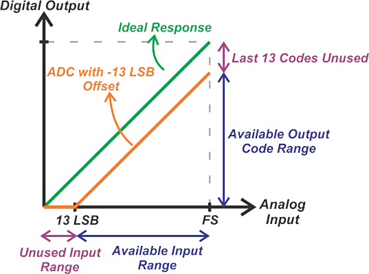
Figure 14. An example showing the negative offset leads to unused input values of the lower end of the nominal input range.
In this case, the ADC has an offset of -13 LSB. However, applying zero volts to the input produces the all-zeros output code, leading to an incorrect offset measurement of zero volts. That’s why with a unipolar ADC, we need a precision voltage in the available input range of the ADC to measure and calibrate the offset error.
To see a complete list of my articles, please visit this page.