Facebook
 Google
 GitHub
 Linkedin
Diode-Based Phase Detectors: Key Principles and Example Circuits
We examine phase detectors that leverage either the nonlinear characteristics or switching capabilities of diodes to perform multiplication.
One effective method for determining the phase difference between two signals involves multiplying the signals and calculating the average of their product. The computed average reflects the phase difference between the signals. This principle is foundational in many phase detection circuits, although the way multiplication is achieved can differ from configuration to configuration. Based on this criterion, we can sort multiplier phase detectors into three categories:
- Gilbert multipliers: As we discussed in the previous article, the basic Gilbert cell utilizes the exponential transfer function of bipolar transistors to achieve multiplication.
- Nonlinear phase detectors: Some phase detectors use a general nonlinear response in conjunction with suitable filtering to perform multiplication in phase detection applications.
- Switching phase detectors: Certain circuits incorporate switching devices along with appropriate filtering to realize multiplication for phase detection purposes.
The latter two phase detector types are often designed using diodes. In this article, we'll take a look at both nonlinear and switching diode-based phase detectors. Let's begin with the most straightforward of these.
The Single-Diode Phase Detector
Figure 1 shows a simple mixer that uses the diode's nonlinearity to determine the phase difference (Δϕ) between the input signals, v1(t) and v2(t).
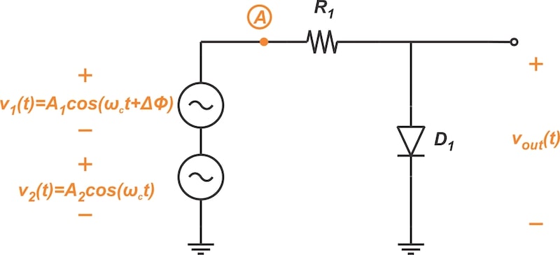
Figure 1. Using a single diode mixer for phase detection.
To understand the circuit's operation, note that the input-output characteristics of memoryless, nonlinear systems can be approximated by a polynomial expression:
$$v_{out}(t) ~\approx~ \alpha_0 ~+~ \alpha_1 v_A(t) ~+~ \alpha_2 (v_A(t))^2 ~+~ \alpha_3 (v_A(t))^3 ~+~ \ldots$$
Equation 1.
where vA(t) represents the voltage applied to the series connection of the diode and resistor. Since the sum of v1(t) and v2(t) is applied to the circuit, we have:
$$v_A(t) ~=~ v_1(t) ~+~ v_2(t)$$
Equation 2.
We are particularly interested in the second-order nonlinearity associated with ⍺2, as it generates the product of v1(t) and v2(t). Applying vA(t) to the nonlinear characteristic, we obtain the output component from the second-order nonlinearity as:
$$\alpha_2 (v_1 ~+~ v_2)^2 ~=~ \alpha_2 \Big( \underbrace{A_1^2 \cos^2(\omega_c t ~+~ \Delta \phi)}_{v_1^2} ~+~ \underbrace{2A_1 A_2 \cos(\omega_c t ~+~ \Delta \phi) \cos(\omega_c t)}_{2v_1v_2} ~+~ \underbrace{A_2^2 \cos^2(\omega_c t)}_{v_2^2} \Big)$$
Equation 3.
Applying basic trigonometric identities, the above expression can be simplified to:
$$\alpha_2 (v_1 ~+~ v_2)^2 \\~=~ \alpha_2 \Big( \underbrace{\frac{A_1^2}{2} [1 ~+~ \cos(2\omega_c t ~+~ 2\Delta \phi)]}_{v_1^2} ~+~ \underbrace{A_1 A_2 [\cos(2\omega_c t ~+~ \Delta \phi)~+~ \cos(\Delta \phi)]}_{2v_1v_2} ~+~ \underbrace{\frac{A_2^2}{2} [1 ~+~ \cos(2\omega_c t)]}_{v_2^2} \Big)$$
Equation 4.
The term corresponding to 2v1v2 includes the sum and difference components of the input sinusoids' arguments. The phase detector is followed by a lowpass filter that removes the sum frequency component, leaving only the difference component. Thus, at the output of the lowpass filter, we have:
$$\alpha_2 (v_1 ~+~ v_2)^2 ~=~ \alpha_2 \Big( \frac{A_1^2 ~+~ A_2^2}{2} ~+~ \underbrace{A_1 A_2 \cos(\Delta \phi)}_{Desired \ Term} \Big)$$
Equation 5.
Note that the lowpass filter also removes the double-frequency components from the v12 and v22 terms.
The second term in Equation 5 represents the desired component, which captures the phase difference between the two input signals. However, the first term is an unwanted DC component that depends on the amplitudes of the input signals. This undesired component, often called the rectification term, can lead to errors in the phase detector.
A balanced configuration can eliminate the rectification term, as we'll see later in this article. Before we explore this further, however, let's discuss the differences between using a single-diode mixer for phase detection and for amplitude modulation.
The Single-Diode Mixer as an AM Modulator
In addition to acting as a phase detector, the single-diode mixer depicted in Figure 1 is capable of producing AM signals. When used as an AM modulator, one of the inputs is the message signal, m(t), and the other is the carrier wave. This is illustrated in Figure 2.
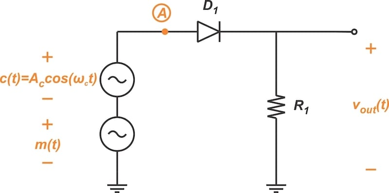
Figure 2. The single-diode modulator.
Even though the diode and resistor positions are reversed compared to the schematic in Figure 1, this doesn't represent a fundamental difference. Both circuits operate on the principle of the diode introducing a second-order nonlinearity, also known as a square-law characteristic.
However, it's important to highlight a key distinction between these two applications: the phase detector's intended output is a DC signal, so the output must be delivered to a lowpass filter to extract the desired signal from the accompanying spectral components. Conversely, the modulator's output is a signal centered around the carrier frequency, necessitating the use of a bandpass filter afterward. For clarity, the block diagram of a typical square-law modulator is shown in Figure 3.
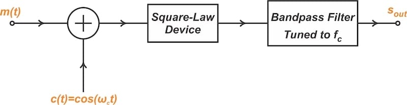
Figure 3. Block diagram of the square-law modulator.
Another difference between the two applications is that while the rectification term interferes with the desired output of the square-law phase detector, it doesn't affect the square-law modulator. This is because the modulator's output is centered around the carrier frequency rather than DC.
A Balanced Configuration of Two Single-Diode Mixers
Shown in Figure 4 is a balanced configuration that can eliminate the rectification term.
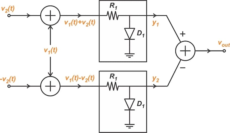
Figure 4. Block diagram of a single-balanced circuit that eliminates the rectification term.
As we can see, the balanced configuration incorporates two identical square-law devices. The output signals from the two nonlinear devices are subtracted from each other to produce the final output. Note that one of the inputs, v2(t), has its sign changed when comparing the upper and lower paths.
From our earlier analysis of the single-diode mixer, we know that the second-order nonlinearity produces the following signal at node y1:
$$\alpha_2 (v_1 ~+~ v_2)^2 ~=~ \alpha_2 \Big( \frac{A_1^2 ~+~ A_2^2}{2} ~+~ \underbrace{A_1 A_2 \cos(\Delta \phi)}_{Desired \ Term} \Big)$$
Equation 6.
To determine the corresponding component generated by the lower path at node y2, we just need to substitute A2 with –A2, leading to:
$$\alpha_2 (v_1 ~-~ v_2)^2 ~=~ \alpha_2 \Big( \frac{A_1^2 + A_2^2}{2} ~-~ \underbrace{A_1 A_2 \cos(\Delta \phi)}_{Desired \ Term} \Big)$$
Equation 7.
By subtracting Equation 7 from Equation 6, we obtain the output component generated by the square-law characteristic:
$$\alpha_2 (v_1 ~+~ v_2)^2 ~-~ \alpha_2 (v_1 ~-~ v_2)^2 ~=~ 2\alpha_2 A_1 A_2 \cos(\Delta \phi)$$
Equation 8.
We can see from this equation that the rectification term doesn't appear at the output.
The configuration in Figure 4 is referred to as single-balanced because the linear term ⍺1 in the characteristic equation allows one of the inputs, v2(t), to appear at the output, as shown below:
$$\alpha_1 (v_1 ~+~ v_2) ~-~ \alpha_1 (v_1 ~-~ v_2) ~=~ 2\alpha_1 v_2$$
Equation 9.
While it is beyond the scope of this article, two of the single-balanced circuits from Figure 4 can be used in a double-balanced configuration to cancel both inputs.
Diode Ring Phase Detector
One popular diode-based phase detector is the diode ring configuration shown in Figure 5.
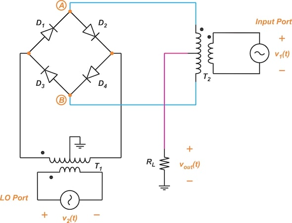
Figure 5. The diode ring phase detector.
Although a fully accurate analysis of this circuit is too complex for this article, we can still gain useful insights by assuming that v2(t) is a square wave large enough to forward-bias the diodes. During the positive half-cycle of v2(t), the diodes D1 and D2 are forward-biased, whereas the diodes D3 and D4 are reverse-biased.
In this case, considering the symmetry of the circuit and noting that the center tap of T1 is grounded, node A should also be at the ground potential. For this to work effectively, diodes D1 and D2 must be well-matched and the transformer's secondary must be accurately center-tapped.
Conversely, during the negative half-cycle of v2(t), diodes D3 and D4 are turned on, and the diodes D1 and D2 are off. In this case, the symmetry of the circuit forces node B to be at the ground potential.
In short, nodes A and B are alternately grounded. This effectively multiplies v1(t) by a square wave that switches between ±1 as it passes through transformer T2 to appear at the output as vout(t). We assume that each half of the center-tapped secondary of T2 has the same number of turns as the primary winding. In other words, the total turns ratio of T2 is 1:2 between the primary and secondary.
Since a 50% duty cycle square wave consists of a fundamental frequency and its odd harmonics, the circuit multiplies v1(t) by sinusoidal components at both the fundamental frequency and the odd harmonics. Just like in the single-diode phase detector, a lowpass filter is necessary to separate the desired signal from unwanted spectral components.
Observations on the Diode Ring Phase Detector
Assume that v1(t) is described by:
$$v_1(t) ~=~ A_1 \cos(\omega_c t~+~ \Delta \phi)$$
Equation 10.
where Δϕ denotes the phase difference between v1(t) and v2(t). The signal produced by the diode ring is the product of v1(t) and the fundamental component of the square wave toggling between ±1. For this square wave, the amplitude of the fundamental component is 4/π. Therefore, the signal at the output of the lowpass filter is given by:
$$v_{d} ~=~ \frac{1}{2}~\times~ \frac{4}{\pi} ~\times~ A_1 \ \cos(\Delta \phi) ~=~ \frac{2}{\pi} ~\times~ A_1 \ \cos(\Delta \phi)$$
Equation 11.
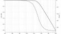
The relationship between the output voltage and the input phase difference exhibits a sinusoidal pattern. This is illustrated in Figure 6.
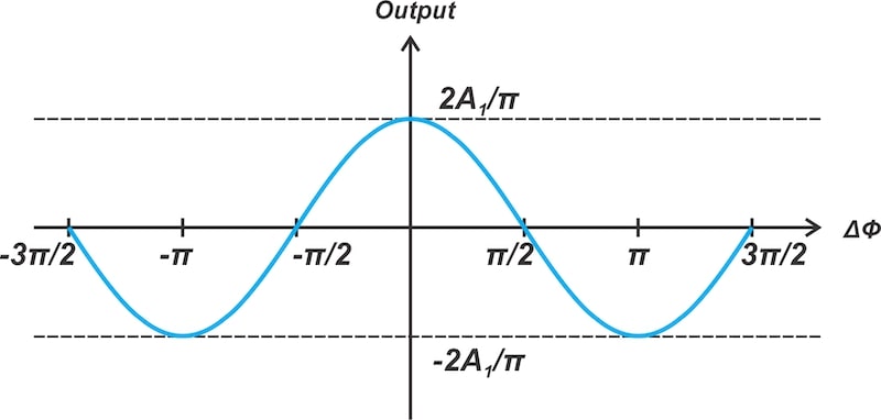
Figure 6. Diode ring phase detector's output vs. input phase error.
Equation 11 shows that the phase detector gain isn't constant and changes with the phase difference (Δϕ). By differentiating vd with respect to the phase difference, we can determine the phase detector gain:
$$k_d ~=~ \frac{d}{d ( \Delta \phi) }v_{d} ~=~- \frac{2A_1}{\pi} \ \sin ( \Delta \phi)$$
Equation 12.
At Δϕ = 0, the gain is zero. At Δϕ = 90 degrees, which corresponds to the locked condition, the phase detector gain reaches its maximum value of |kd| = 2A1/π.
The diode ring phase detector can function with waveforms of any shape. However, assuming that one of the inputs is a sufficiently large square wave is what enables a simplified analysis.
It should be noted that, like the single-diode mixer, the diode ring configuration can also serve as an AM modulator. In this case, a bandpass filter tuned to the carrier frequency is needed at the output to isolate the desired component.
Other Diode-Based Phase Detectors
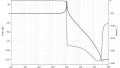
The range of diode-based phase detectors isn't confined to those discussed above. A review of the available literature will reveal other phase detector circuits, including the two examples illustrated in Figure 7.
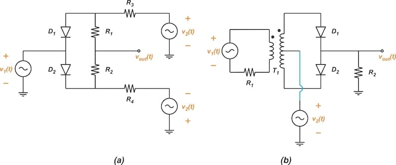
Figure 7. Two more examples of diode-based phase detectors.
Owing to space limitations, we won't cover these circuits in this article. Readers who are interested can refer to the books 'Phase-Locked Loops: Application to Coherent Receiver Design' by A. Blanchard and 'Phase-Lock Basics' by W. Egan.
Wrapping Up
Diode-based phase detectors leverage either the nonlinearity or switching behavior of the diode to perform multiplication and, ultimately, phase detection. In this article, we presented several examples of these phase detectors. With these circuits, the relationship between the output voltage and the input phase difference typically displays a sinusoidal pattern.
Notably, the diode ring phase detector can operate at frequencies much higher than those of transistor phase detectors. Its range extends well into the microwave domain. This circuit has been widely sold at a low cost under the name 'double-balanced mixer.' It provides good performance and requires little effort from the PLL designer.
Finally, it's important to highlight that the phase detectors mentioned above are closely related to mixers and modulators. Many of these circuits can actually be utilized as modulators, mixers, or phase detectors, depending on the desired application.
All images used courtesy of Steve Arar
Related Content