 Facebook
 Google
 GitHub
 Linkedin
Introduction to Phase/Frequency Detectors
Learn how using a phase/frequency detector (PFD) in place of a phase detector improves the acquisition range of a PLL.
When studying the fundamentals of phase-locked loops (PLLs), we start with how a phase detector can guide the loop to lock. In practice, however, many PLL implementations opt for a phase/frequency detector (PFD) over a phase detector. The PFD is a popular sequential circuit that can identify differences in both phase and frequency between its two inputs. As we'll see in this article, it provides a better acquisition range than a circuit that only detects the phase difference.
Limited Acquisition Range of Phase Detectors
Shown in Figure 1 is a basic PLL.
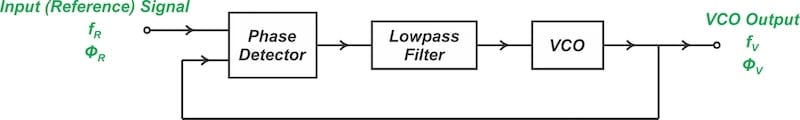
Figure 1. The basic PLL configuration using a phase detector.
Detecting the phase difference between the input (or reference) signal and the VCO output is a vital part of the PLL's operation. In my series on PLL design, a phase detector was therefore part of every configuration we examined. However, it's important to note that a phase detector restricts the loop's acquisition range. In other words, with a phase detector, a substantial difference between the VCO output frequency (fV) and the input frequency (fR) could prevent the loop from locking.
To grasp this limitation, consider the Gilbert-cell phase detector. As you may recall, the phase detector generates the difference frequency (fR – fV) at its output. When fR – fV is relatively high, the signal is attenuated by the subsequent lowpass filter.
The larger the frequency separation between fR and fV, the more pronounced the attenuation from the filter becomes. This makes it harder for the loop to detect the frequency difference. In essence, when fR is far from fV, the signal generated at the output of the lowpass filter is too weak to drive the VCO in the correct direction.
What About Using a Frequency-Locked Loop Instead?
Because phase detectors provide minimal information when there is a substantial difference between input frequencies, they cannot guarantee that the loop will always achieve lock. Enhancing the acquisition range requires a circuit capable of detecting the frequency difference between the inputs. This concept is illustrated in Figure 2.
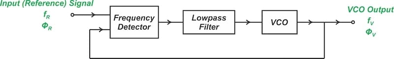
Figure 2. A frequency-locked loop.
Note that the loop employs a frequency detector rather than a phase detector. Along with the lowpass filter, it generates a DC signal that reflects the difference between fR and fV. In this way, the VCO is driven toward minimizing the frequency difference even if fR and fV are far apart.
However, frequency detectors have a major limitation: they cannot guarantee that fR will eventually equal fV. This can be caused by either the finite loop gain or the offsets in the frequency detector circuit. This behavior resembles that of an op amp set up in a unity-gain feedback configuration. Such an op amp is unable to reduce the voltage difference at its inputs to zero because of the finite loop gain and/or inherent op amp offsets.
We Need Phase Detectors to Equalize the Input and Output Frequencies
The configuration in Figure 1, which utilizes a phase detector, comes closer to equalizing the input and output frequencies. However, this isn't the same as ensuring this difference is zero. After the loop settles, a small constant phase difference of ϕe may exist between the input and output phases:
$$\phi_R~=~\phi_V~+~\phi_e$$
Equation 1.
Despite this non-zero phase difference, the circuit in Figure 1 guarantees that the input frequency (fR) equals the output frequency (fV). This can be understood by recognizing that instantaneous frequency is the derivative of phase. Because ϕe is a constant, when we take the derivative of Equation 1, it vanishes.
Consequently, even with a constant phase difference between the input and output signals, the circuit can still equalize the input and output frequencies. In other words, when the input and output phases are locked, the frequencies must also be equal.
To summarize, although a frequency detector improves the acquisition range, it can't equalize the input and output frequencies. For that, we need a phase detector. Consequently, the loop requires a circuit that functions as a frequency detector when the input frequencies differ and as a phase detector when they are identical. This type of circuit, which we will discuss in the rest of the article, is known as a phase/frequency detector (PFD).
Basics of the Phase/Frequency Detector
Shown in Figure 3 is a common implementation of the PFD. It uses a pair of D-type flip-flops and an AND gate in a feedback configuration to produce the reset signal.
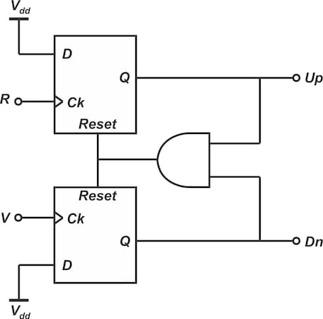
Figure 3. Phase/frequency detector.
The data terminals of the flip-flops are permanently driven to a logic HIGH. The labels R and V indicate the input signal and the signal generated by the VCO, respectively. The input signals are applied to the clock terminals of the flip-flops. The output from one of the flip-flops is labeled Up, while the other flip-flop's output is labeled Dn (short for 'Down').
When a rising edge occurs on R or V inputs, their corresponding flip-flop's output goes HIGH. If both Up and Dn are HIGH simultaneously, the AND gate resets the flip-flops.
Typical Waveforms When Inputs Have Identical Frequencies
Figure 4 shows the typical waveforms for the PFD when both inputs are at the same frequency, with R leading V.
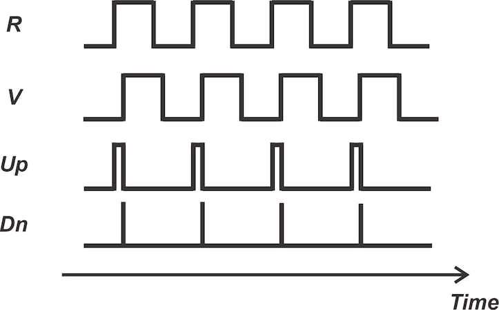
Figure 4. Typical waveforms of the PFD when both inputs are at the same frequency and R leads V.
The upper flip-flop goes HIGH first because the rising edge of the R input occurs before that of the V input. It remains in the logic-HIGH state until the rising edge of the V input activates the Dn output. This resets flip-flops. Note that the pulses at the Dn output are quite narrow, as the logic-HIGH state of this output triggers the reset path.
Figure 5 shows the typical waveforms when the V pulse leads the R input.

Figure 5. Typical waveforms when the V input is ahead of the R input.
An active Up output indicates to the PLL that the VCO is lagging behind the input signal and needs to boost its frequency. This is what we see in Figure 4. The active Dn output shown in Figure 5 indicates the opposite, directing the loop to lower the VCO frequency. In this way, the active Up or Dn outputs provide information about the direction of phase error.
The width of the pulses at the active output tells us the magnitude of the phase error. When R and V pulses are in perfect phase alignment, both flip-flops will go HIGH simultaneously and reset at the same time. This creates the narrow pulses shown in Figure 6.
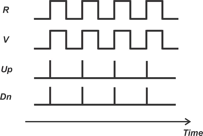
Figure 6. Typical waveforms when the R and V pulses are in perfect phase alignment.
With the PFD, the final output is obtained by subtracting the Dn output from the Up output. Figure 7 shows a configuration that generates the final output using an op amp subtractor.
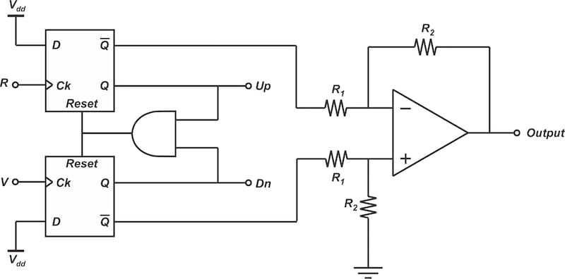
Figure 7. A PFD incorporating an op amp circuit to generate the final output.
Since the final output is derived from the difference between the Up and Dn outputs, the narrow pulses created when the inputs are in phase (Figure 6) would ideally have no impact on circuit performance. In practice, however, these narrow pulses contribute to increased ripple on the VCO control voltage.
Typical Waveforms When Inputs Have Different Frequencies
Next, let's consider what happens when the reference frequency is greater than the VCO frequency (fR > fV). Figure 8 shows the example waveforms for this scenario.
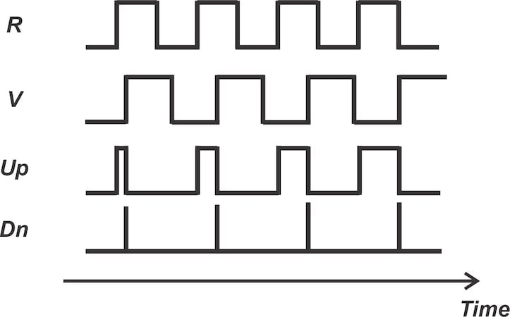
Figure 8. Typical waveforms when fR > fV.
As observed, the Up output is triggered by a rising edge from the higher-frequency input and remains active until a rising edge occurs on the lower-frequency input. The duty cycle of the Up output is an indication of the frequency difference between the inputs. When fR < fV, the Dn output is activated, indicating that the VCO frequency should be lowered to achieve lock. This shows that the circuit can detect both phase and frequency difference between the inputs.
Input-Output Characteristic of the PFD
The average PFD output—which is to say, the difference of the Up and Dn outputs—is a function of the input phase difference. It behaves as shown in Figure 9.
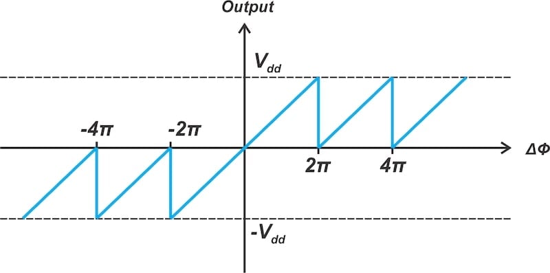
Figure 9. The PFD's input-output characteristic.
The linear range of operation extends over 4π radians, with a constant gain of:
$$k_d~=~\frac{V_{dd}}{2 \pi}$$
Equation 2.
The gain is the same as that of the RS flip-flop phase detector. From Figure 9, it is evident that the lock point must be set at zero degrees to achieve the maximum lock range.
Wrapping Up
The PFD has a linear range of ±2π radians. During the initial phase of a transient, it functions as a frequency detector, adjusting the VCO frequency to align with the input frequency. Once the two frequencies are sufficiently close, the PFD begins to operate as a phase detector, achieving phase lock in the loop. This enables us to overcome the issue of limited acquisition range in phase detectors, guaranteeing that the PLL will always achieve lock.
If you're interested in learning more about PLLs that use phase/frequency detectors, I recommend the following two books:
- "Design of CMOS Phase-Locked Loops From Circuit Level to Architecture Level" by Behzad Razavi.
- "Phase-locked Loop Circuit Design" by Dan H. Wolaver.
All images used courtesy of Steve Arar
Related Content


Quite interesting
I recall implementing one of these in a 22v10, years ago. I found it had a metastable mode where if the imputs lined up just right it would rapidly oscillate by itself. Had to go to a different type of detector to get stable performance.