 Facebook
 Google
 GitHub
 Linkedin
Foundations for PLL Nonlinear Analysis: Modeling the Phase Detector and VCO
The phase-locked loop (PLL) is widely used in contemporary analog and digital communication systems. In this article, we develop a nonlinear model for the analog PLL by analyzing its key components.
The phase-locked loop (PLL) is a negative feedback system capable of tracking the phase and frequency of the carrier component of an incoming signal. This functionality makes PLLs useful for synchronous demodulation of AM signals with a suppressed carrier, among other things. In FM systems, PLL-based demodulators often achieve superior noise performance compared to other options, especially in noisy channels. PLLs are also employed for frequency synthesis and as core components in numerous digital demodulators.
To gain a clear understanding of the PLL's operation, we need to construct a mathematical model for the system. In this article—the first in a new series exploring the essentials of PLL operation—we'll focus on developing a nonlinear model for analog PLLs. In the process, we'll also develop models for the multiplier phase detector and voltage-controlled oscillator (VCO). This discussion will lay the groundwork for the next article in the series, which examines the behavior of a first-order PLL in acquisition mode.
Basics of the PLL
The block diagram of a simple PLL is shown in Figure 1.
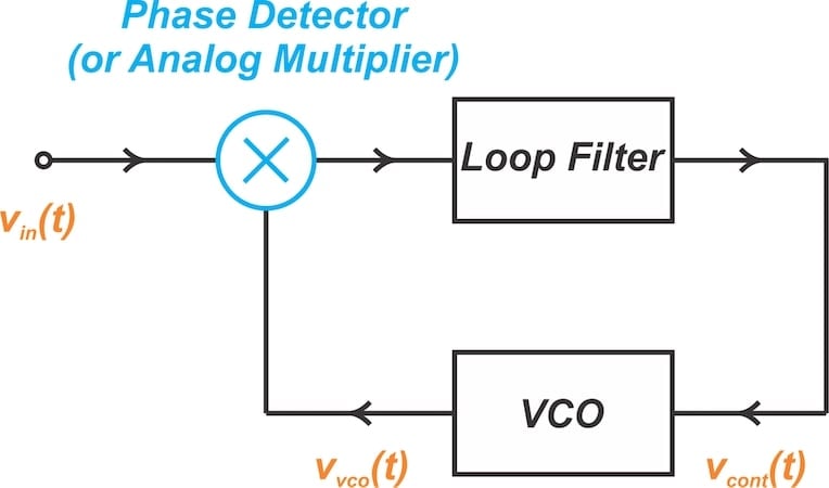
Figure 1. Basic block diagram of a PLL.
As you may recall from our discussion of FM demodulation using a PLL, a phase-locked loop has three key components:
- A phase detector.
- A lowpass filter.
- A VCO.
These are arranged in a feedback loop. The phase detector compares the phase of the input signal with the phase of the VCO output, generating a signal that varies with the phase difference. This signal then passes through a lowpass filter, producing the VCO's control voltage.
The feedback configuration forces the VCO to change frequency in the direction that reduces the phase difference between the VCO and the input signal. When the VCO phase and frequency follow the input sufficiently closely, we say that the VCO is locked with the input frequency.
To gain a clearer understanding of PLL operation, we must construct a mathematical model for the system. We'll start by developing a model for the phase detector.
The Ideal Phase Detector
A phase detector generates an output signal that is proportional to the phase difference between its two input signals. Therefore, the ideal phase detector output (vout) may be described as:
$$v_{out} ~=~ k_d \big ( \phi_1 ~-~ \phi_2 \big)$$
Equation 1.
where:
ϕ1 is the phase of the first input
ϕ2 is the phase of the second input
kd is the phase detector gain in V/rad.
From Equation 1, we see that an ideal phase detector will have a linear response. Practical phase detectors often exhibit nonlinear input-output characteristics that repeat cyclically. However, we can assume a linear relationship within a narrow phase range around the loop's lock point. The gain of the phase detector may be defined as the slope of the characteristic at this point.
The Multiplier Phase Detector
There are several different methods of implementing a phase detector. In PLLs where both the input and the VCO output are sinusoidal waves, the most commonly used phase detector is an analog multiplier followed by a lowpass filter. This arrangement is illustrated in Figure 2.

Figure 2. A phase detector built around an analog multiplier.
Often, a Gilbert cell is used to implement the analog multiplier.
Consider applying two sinusoids with the same frequency (ωc) but different phases to the above circuit, defined as:
$$v_1 ~=~ A_1 \cos(\omega_c t~+~ \phi_1) \quad \text{and} \quad v_2 ~=~ A_2 \cos(\omega_c t~+~ \phi_2)$$
Equation 2.
Using a basic trigonometric identity, the signal at the output of the multiplier is obtained as:
$$v_3 ~=~ \frac{1}{2}A_1 A_2 \big [ \cos(2\omega_c t~+~ \phi_1 ~+~ \phi_2) ~+~ \cos(\phi_1 ~-~ \phi_2) \big ]$$
Equation 3.
The output includes components corresponding to both the sum and the difference of the input sinusoids' arguments. The lowpass filter following the multiplier removes the sum frequency component, leaving only the difference component. Thus, at the output of the lowpass filter, we have:
$$v_{out} ~=~ \frac{1}{2}A_1 A_2 \ \cos(\phi_1 ~-~ \phi_2)$$
Equation 4.
For a given phase difference, the output of the phase detector is therefore a DC term.
The phase detector output varies sinusoidally with the phase difference, as shown in Figure 3.

Figure 3. The output of a multiplier phase detector.
Assuming that the loop gain is high, the PLL locks when the phase detector output is zero. Thus, with a multiplier phase detector, the loop locks when the phase difference between the PLL input and the VCO output is 90 degrees. For this reason, a multiplier phase detector is often called a quadrature phase detector.
By differentiating Equation 4 with respect to the phase difference (Δϕ), we can determine the phase detector gain:
$$k_d ~=~ \frac{d}{d \phi}v_{out} ~=~- \frac{1}{2} A_1 A_2 \ \sin ( \Delta \phi)$$
Equation 5.
Note that the phase detector gain is a function of the phase difference. At Δϕ = 0, the gain is zero; when the loop locks at Δϕ = 90 degrees, the phase detector gain reaches its maximum value of:
$$k_d \Big \vert_{\Delta \phi = \pi/2} ~=~- \frac{1}{2} A_1 A_2$$
Equation 6.
Within any 2π interval, there are two distinct phase angles that result in a zero output from the phase detector. For instance, in the interval from –π to π, the output is zero at both –π/2 and π/2. The key questions are: which of these two points will the loop lock onto? Is it possible to achieve lock at both points?
To answer these, we need to understand that the gain (or slope) of the input-output characteristic is positive at one point and negative at the other. Depending on the sign of the gain of other components within the PLL feedback path, one point will result in a negative feedback system, while the other will create a positive feedback system.
The PLL will lock to the point associated with the negative feedback system. The other point is metastable. Therefore, the PLL will not lock to that point.
Modeling a Multiplier Phase Detector
From the above explanation, we know that in the lock condition, a multiplier phase detector results in a 90-degree phase difference between the input and the VCO output. Taking this into account lets us simplify our notation a bit when developing a model for the multiplier phase detector. If the PLL input is denoted by:
$$v_1 ~=~ A_1 \cos(\omega_c t~+~ \phi_1)$$
Equation 7.
We may express the VCO output as:
$$v_2 ~=~ A_2 \cos(\omega_c t~+~ \phi_2 ~+~ \frac{\pi}{2}) ~=~ -A_2 \sin(\omega_c t~+~ \phi_2)$$
Equation 8.
With this new definition, the phase angles ϕ1 and ϕ2 will be equal when the PLL locks. If we multiply v1 by v2 and filter out the double-frequency component, we obtain the phase detector output as:
$$v_{out}~=~\frac{1}{2}A_1 A_2 \sin(\phi_1~-~\phi_2)$$
Equation 9.
Using the above equation, we can develop a model for the multiplier phase detector. This model is shown in Figure 4.

Figure 4.The multiplier phase detector model.
The phase detector model operates on the input phase angles (ϕ1 and ϕ2) rather than the input signals (v1 and v2). If we know the frequency of operation (ωc), knowledge of ϕ1 and ϕ2 fully determines the input signals.
This model accounts for the nominal 90-degree phase difference we discussed earlier. Therefore, when the lock condition is achieved, we have ϕ1 = ϕ2.
From Equation 9, the gain of the phase detector is a function of the input signal amplitude (A1). Therefore, designing a PLL requires knowledge of the input signal level, which varies over time. To address this issue, a hard limiter may be employed at the input of the PLL.
We sometimes incorporate an additional gain factor in the above model to account for the gain of the multiplier circuit and/or the following lowpass filter.
Modeling the Voltage-Controlled Oscillator (VCO)
Before we can analyze a PLL, we also need to develop a model for the VCO. The VCO output frequency is offset from its free-running frequency (ωc) by an amount proportional to the VCO's control voltage (vcont). Mathematically, the output frequency may be expressed as:
$$\omega_{vco} ~=~ \omega_c ~+~ k_{vco} v_{cont}$$
Equation 10.
where kvco is the VCO gain factor measured in radians per second per volt (rad/sV). This unit of measurement is suitable for PLL calculations because of its compatibility with the phase detector gain, measured in V/rad.
Equation 10 gives the instantaneous frequency of the VCO. Frequency is the time derivative of phase. Therefore, integrating Equation 10 yields the total phase, which is the argument of the VCO output sinusoid:
$$\phi_{total} ~=~ \omega_{c} t ~+~ k_{vco} \int_0^{t} v_{cont} \ dt$$
Equation 11.
When analyzing PLLs, we're only concerned with the argument's second term, which is called the excess phase. This is consistent with our discussion of phase detector modeling, where we observed that the phase detector operates on the phase angles of its inputs. The excess phase (ϕex) at the VCO output is:
$$\phi_{ex} ~=~ k_{vco} \int_0^{t} v_{cont} \ dt$$
Equation 12.
Using the above equation, we can develop a time-domain model for a VCO. This model is shown in Figure 5.

Figure 5. The VCO model.
Note that the input is a voltage, whereas the output is a phase quantity. A subtle point here is that the VCO's frequency changes almost instantaneously with the input control voltage (see Equation 10). However, the VCO's output phase involves an integral (Equation 12) and so remembers its past values.
By taking the Laplace transform of Equation 12, we obtain the VCO's transfer function in the frequency domain:
$$H(s) ~=~ \frac{\Phi_{ex}}{V_{cont}}(s) ~=~ \frac{k_{vco}}{s}$$
Equation 13.
Putting It All Together
Now that we have models for both the multiplier phase detector and VCO, we can put them together to derive a model for the complete PLL system (Figure 6).
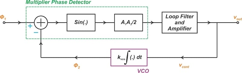
Figure 6. The nonlinear model of a PLL with a multiplier phase detector.
In the next article, we'll use this model to analyze the behavior of the first-order PLL in acquisition mode.
This article is Part 1 of a 12-part series on loop filters in PLL design. All articles in this series are listed below in order of publication:
- Foundations for PLL Nonlinear Analysis: Modeling the Phase Detector and VCO
- Analyzing a First-Order PLL in Acquisition Mode With a Nonlinear Model
- Analyzing First-Order PLLs Using Linear Models
- Understanding the Limitations of the First-Order PLL
- Introduction to Second-Order Type-1 PLLs
- Understanding the Limitations of the Second-Order Type-1 PLL With a Lag Filter
- Analyzing the Lag Filter’s Effect on PLL Performance
- Introducing the Lag-Lead Filter
- Exploring the Bode Plots of PLLs With a Lag-Lead Loop Filter
- Understanding the Time-Domain Response of PLLs With Lag-Lead Filters
- Introduction to Second-Order Type-2 PLLs
- Second-Order Type-2 PLLs: Bode Diagrams, Bandwidth, and Overshoot
All images used courtesy of Steve Arar


Thank you for the well-written article