Facebook
 Google
 GitHub
 Linkedin
Introduction to Second-Order Type-2 PLLs
This article explains how Type-2 PLLs with an integrator loop filter outperform Type-1 systems. To do so, we'll examine the PLL behavior for frequency step and frequency ramp inputs.
The design of the loop filter transfer function in a phase-locked loop (PLL) significantly influences its ability to track and acquire signals. Previously, we learned that a Type-1 PLL exhibits non-zero steady-state error in response to a frequency step and fails to track a frequency ramp.
In this article, we'll explore how a Type-2 PLL can provide better performance in terms of steady-state phase error. As we'll see, a Type-2 loop has zero phase error in response to a frequency step and can track a frequency ramp input with a constant phase error.
Steady-State Errors of Type-1 PLLs: A Review
The linear model of a basic PLL is shown in Figure 1.
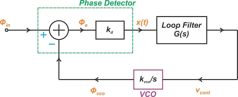
Figure 1. Linear model of a basic PLL.
In previous articles of this series, we used this model to analyze the following PLL configurations:
- The first-order PLL without a loop filter (G(s) = 1).
- The second-order PLL with a lag filter.
- The second-order PLL with a lag-lead filter.
All of these are Type-1 PLLs, meaning that they incorporate a single integrator in their open-loop transfer function. Table 1 shows the steady-state phase errors exhibited by Type-1 PLLs for various types of inputs. Note that K0 = kdkvco is the DC loop gain.
Table 1. Steady-state error of Type-1 PLLs for various input types.
|
|
Phase Step (Δϕ)
rad |
Frequency Step (Δf)
Hz |
Frequency Ramp (R)
Hz/s |
| Type-1 Phase Error | 0 | 2πΔf/K0 | ∞ |
If the input frequency applied to the Type-1 PLL is not equal to the VCO's free-running frequency, the loop adjusts the VCO's control voltage to synchronize it with the input frequency. Even though the VCO ultimately reaches the same frequency as the input, a phase difference remains between them. We'll delve deeper into this behavior in the following section.
Limitations of Type-1 PLLs in Tracking Frequency Steps
When we apply a frequency step, a non-zero control voltage is needed to adjust the VCO to the correct frequency. As shown in Figure 1, the control voltage is derived by multiplying the phase detector output by the DC gain of the loop filter. A non-zero control voltage therefore means the phase detector output is also non-zero.
This implies that a non-zero phase error must be present between the phase detector inputs, making it impossible for a Type-1 PLL to track a frequency step with zero phase error. To overcome this limitation, we require a loop filter with infinite DC gain to generate a non-zero control voltage from a zero phase detector output.
However, the loop filter must provide infinite gain only at DC, rather than at all frequencies. This is essential because one of the loop filter's roles is to reduce high-frequency noise and disturbances. Furthermore, increasing the loop gain at all frequencies would increase the loop bandwidth, which can result in instability.
To provide infinite DC gain, the loop filter should incorporate an integrator. This will result in a pole at the origin. The VCO also includes an integrator, bringing the total number of integrators in the loop to two. This classifies the loop as a Type-2 system.
Second-Order Type-2 PLL
The basic second-order Type-2 PLL uses the following loop filter:
$$G(s) ~=~ \frac{1 + s/\omega_z}{s} ~=~ \frac{1}{s} ~+~ \frac{1}{\omega_z}$$
Equation 1.
where ωz is a positive value. Such a loop filter feeds back the phase error and its integral to the VCO input. In control theory, this approach is called proportional-integral (PI) feedback.
As we'll see, the zero of the loop filter introduces a positive phase shift to the open-loop transfer function, counteracting some of the negative phase shift caused by the two integrators and thereby stabilizing the loop.
Based on Figure 1, the closed-loop transfer function from ϕin to ϕvco for a Type-2 PLL is obtained as:
$$H(s) ~=~ \frac{\phi_{vco}}{\phi_{in}} (s) ~=~ \frac{K_0(1 ~+~ s/\omega_z)}{s^2~+~K_0s/ \omega_z~+~K_0}$$
Equation 2.
As mentioned in earlier articles, it's common in the analysis of second-order systems to represent the denominator of this equation in the standard control theory form. Utilizing this framework, we can rewrite the equation as follows:
$$H(s) ~=~ \frac{2 \zeta \omega_n s ~+~ \omega_n^2}{s^2~+~ 2 \zeta \omega_n s ~+~ \omega_n^2}$$
Equation 3.
where ωn, the natural frequency, is:
$$\omega_n ~=~ \sqrt{K_0}$$
Equation 4.
and ζ, the damping factor, is:
$$\zeta ~=~ \frac{\sqrt{K_0}}{2 \omega_z}$$
Equation 5.
The phase error function, defined as the transfer function from ϕin to ϕe, is shown in Equation 6:
$$H_e(s) ~=~ \frac{\phi_{e}}{\phi_{in}} (s) ~=~ 1 ~-~ H(s) ~=~ \frac{s^2}{s^2~+~ 2 \zeta \omega_n s ~+~ \omega_n^2}$$
Equation 6.
Equations 3 and 6 can be used to determine the output phase and phase error for an arbitrary input.
Error in Response to a Frequency Step
Next, let's use the final-value theorem to determine the steady-state error of a Type-2 PLL in response to a step change in the input frequency. According to the final-value theorem, if x(t) is a time-domain function and X(s) is its Laplace transform, then the final value of x(t) as t tends to infinity can be found using the following formula:
$$\lim_{t\to \infty} x(t) ~=~ \lim_{s \to 0} sX(s)$$
Equation 7.
Let's assume that the input frequency shifts by Δf Hz. Since phase is the integral of angular frequency over time, a frequency step of Δf results in the input phase changing in the following ramp function:
$$\phi_{in}(t) ~=~ (2 \pi \Delta f ~\times~ t) \ u(t) ~\xrightarrow{\text{Laplace}}~ \phi_{in}(s) ~=~ \frac{2 \pi \Delta f}{s^2}$$
Equation 8.
where u(t) is the unit step function.
Substituting ϕin(s) into the error transfer function (Equation 6) and applying the final-value theorem, the steady-state phase error for a frequency step is obtained as:
$$\lim_{t \to \infty} \ {\phi_e (t)} ~=~ \lim_{s \to 0} \ s{\phi_e}(s) ~=~ \lim_{s \to 0} \ s ~\times~ \frac{s^2}{s^2~+~ 2 \zeta \omega_n s ~+~ \omega_n^2} ~\times~ \frac{2 \pi \Delta f}{s^2} ~=~ 0$$
Equation 9.
Thus, unlike a Type-1 PLL, a Type-2 PLL can track a frequency step with zero steady-state error. To better visualize this, we can substitute ϕin(s) into the error transfer function (Equation 6). We then obtain the phase error in the time domain, ϕe(t), by taking the inverse Laplace transform.
Instead of finding the inverse Laplace transform analytically, we can also use software packages like Matlab to generate the corresponding time-domain waveform. Figure 2 shows the phase error generated by Matlab for Δf = 1 Hz, ωn = 1 rad/s, and ζ = 0.3, 0.7, and 2.0.
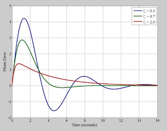
Figure 2. The phase error of the Type-2 PLL in response to a frequency step.
Even though the value of ζ impacts the oscillations, the curves will eventually approach zero if allowed enough time.
Error in Response to a Frequency Ramp
To analyze the steady-state error in response to a frequency ramp, we assume that the input frequency changes linearly over time at a rate of R. Noting once again that phase is the integral of angular frequency over time, we obtain the input phase equation:
$$\phi_{in}(t) ~=~ 2 \pi \int_0 ^t Rt \ dt ~=~ \pi R t ^2 \ u(t) ~\xrightarrow{\text{Laplace}}~ \phi_{in}(s) ~=~ \frac{2 \pi R}{s^3}$$
Equation 10.
Substituting ϕin(s) into the error transfer function (Equation 6) and applying the final-value theorem yields the steady-state phase error for a frequency ramp, as shown below:
$$\lim_{t \to \infty} \ {\phi_e (t)} ~=~ \lim_{s \to 0} \ s{\phi_e}(s) ~=~ \lim_{s \to 0} \ s ~\times~ \frac{s^2}{s^2~+~ 2 \zeta \omega_n s ~+~ \omega_n^2} ~\times~ \frac{2 \pi R}{s^3} ~=~ \frac{2 \pi R}{\omega_n^2}$$
Equation 11.
From Equation 4, we know that ωn squared equals the DC loop gain (ωn2 = K0). Therefore, the steady-state error in response to a frequency ramp at a rate of R Hz/s is directly proportional to the slope of the frequency ramp and inversely proportional to the DC loop gain.
Figure 3 shows the phase error generated by Matlab for R = 1 Hz/s, ωn = 1 rad/s, and ζ = 0.3, 0.7, and 2.0.
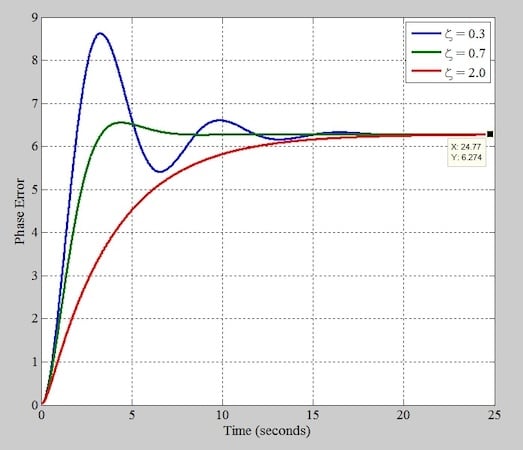
Figure 3. The phase error of the Type-2 PLL in response to a frequency ramp.
Note that the final error value is 2πR/K0 = 2π = 6.28 radians. The error can be reduced by increasing the loop gain.
We can use the PLL transfer function given in Equation 3 to calculate the output phase (ϕvco). By taking the time derivative of ϕvco, we obtain the output frequency. To demonstrate how the output frequency follows the input frequency, Figure 4 presents the output frequency for R = 1 Hz/s, ωn = 1 rad/s, and ζ = 0.7.
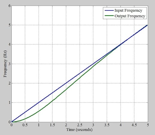
Figure 4. The Type-2 PLL's input frequency (blue) and output frequency (green) when the input is a frequency ramp.
Table 2 lists our findings on the steady-state errors of Type-2 PLLs for various inputs. For ease of comparison, the results for Type-1 PLLs are also included.
Table 2. The steady-state errors of Type-1 and Type-2 PLLs for various input types.
|
|
Phase Step (Δϕ)
rad |
Frequency Step (Δf)
Hz |
Frequency Ramp (R)
Hz/s |
| Type-1 Phase Error | 0 | 2πΔf/K0 | ∞ |
| Type-2 Phase Error | 0 | 0 | 2πR/K0 |
Example: Determining the Loop Gain of a Second-Order Type-2 PLL
A Type-2 PLL is to be designed to have a steady-state phase error of 3 × 10⁻⁵ radians in response to a frequency ramp with a slope of R = 1 Hz/s. Calculate the required DC loop gain to accomplish this.
The steady-state error in response to a frequency ramp is given by:
$$\phi_e(t~=~\infty) ~=~ \frac{2 \pi R}{K_0}$$
Equation 12.
Substituting ϕe = 3 × 10⁻⁵ radians and R = 1 Hz/s into this equation and solving for K0, we obtain the loop gain:
$$K_0~=~\frac{2 \pi~\times~1 ~\text{Hz/s}}{3~\times~10^{-5}~\text{radians}}~=~2.09~\times~10^5~\text{(rad/s)}^2$$
Equation 13.
Wrapping Up
In comparison to a Type-1 PLL, a Type-2 PLL reduces the steady-state phase error. A Type-2 loop has zero phase error in response to a frequency step and tracks a frequency ramp input with a constant phase error that can be reduced by incorporating a higher DC loop gain. By extending this analysis, it's possible to show that a Type-3 loop can track a frequency ramp with no phase error. However, Type-3 PLLs are beyond the scope of our current discussion.
In the following article, we'll further investigate the Type-2 second-order PLL to uncover its other performance aspects. This will aid us in making informed choices about the loop parameters.
This article is Part 11 of a 12-part series on loop filters in PLL design. All articles in this series are listed below in order of publication:
- Foundations for PLL Nonlinear Analysis: Modeling the Phase Detector and VCO
- Analyzing a First-Order PLL in Acquisition Mode With a Nonlinear Model
- Analyzing First-Order PLLs Using Linear Models
- Understanding the Limitations of the First-Order PLL
- Introduction to Second-Order Type-1 PLLs
- Understanding the Limitations of the Second-Order Type-1 PLL With a Lag Filter
- Analyzing the Lag Filter’s Effect on PLL Performance
- Introducing the Lag-Lead Filter
- Exploring the Bode Plots of PLLs With a Lag-Lead Loop Filter
- Understanding the Time-Domain Response of PLLs With Lag-Lead Filters
- Introduction to Second-Order Type-2 PLLs
- Second-Order Type-2 PLLs: Bode Diagrams, Bandwidth, and Overshoot
All images used courtesy of Steve Arar
Related Content