Facebook
 Google
 GitHub
 Linkedin
Introduction to Second-Order Type-1 PLLs
Learn how adding a lowpass loop filter to a PLL with a single integrator impacts both the frequency-domain and time-domain response.
In the previous installment of this series, we learned that the first-order phase-locked loop (PLL) exhibits a non-zero steady-state phase error when responding to a frequency step. We also discovered that minimizing the steady-state error comes at the expense of noise performance.
A first-order PLL does not include a loop filter. In this article, we'll explore a slightly more complex setup: the second-order Type-1 PLL, which utilizes a straightforward first-order loop filter. After introducing this configuration, we'll analyze how the loop filter influences the PLL's response in both the time and frequency domains.
Why Is a Loop Filter Required?
Before we examine the effects of adding a loop filter, let's establish why we need one. The linear model of an analog PLL is shown in Figure 1.
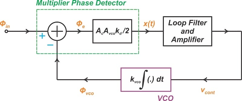
Figure 1. Linear model of a PLL with a multiplier phase detector.
The VCO's output frequency is determined by its control voltage. Disturbances and noise on the control voltage can harm the loop's performance. Using a loop filter enhances performance by reducing these unwanted fluctuations.
For example, a multiplier phase detector's output may only vary by a few hundred millivolts, requiring an extra loop amplifier to boost the signal for the VCO. However, the amplifier introduces noise, so a loop filter is needed to limit the noise bandwidth. This loop filter serves to limit the noise from other sources as well.
Furthermore, the output of a digital phase detector generally contains repetitive pulses that disturb the VCO. The loop filter can suppress the high-frequency components of the phase detector output, cleaning up the VCO output signal.
Without a loop filter, the PLL's performance is entirely governed by the loop gain. No other parameters are available to control the loop behavior. Incorporating a loop filter introduces additional design parameters, allowing us better control over the following performance metrics:
- Steady-state error.
- Loop bandwidth.
- Noise performance.
- Transient response.
We'll discuss these metrics further in the next article.
The Second-Order Type-1 PLL
Consider a lowpass loop filter with a transfer function given by:
$$G(s) ~=~ \frac{1}{1~+~ s / \omega_f} ~=~ \frac{\omega_f}{ s ~+~ \omega_f}$$
Equation 1.
where ωf denotes the loop filter's cutoff frequency. We often call this setup a PLL with a lag filter to clarify the particular configuration of the loop filter.
Using the diagram in Figure 1, it can be easily shown that the transfer function of this PLL from the input phase (ϕin) to the output phase (ϕvco) is:
$$H(s) ~=~ \frac{\phi_{vco}}{\phi_{in}} (s) ~=~ \frac{K_0 \omega_f}{s^2 ~+~ \omega_f s ~+~ K_0 \omega_f}$$
Equation 2.
When working with second-order systems, we usually express the denominator in the standard control theory form, producing:
$$H(s) ~=~ \frac{\omega_n ^2}{s^2 ~+~ 2 \zeta \omega_n s ~+~ \omega_n^2}$$
Equation 3.
where ωn is the natural frequency, given by:
$$\omega_n ~=~ \sqrt{K_0 \omega_f}$$
Equation 4.
and ζ is the damping factor:
$$\zeta ~=~ \frac{1}{2} \sqrt{\frac{\omega_f}{K_0}}$$
Equation 5.
Equation 3 shows that when using a simple lowpass loop filter, the closed-loop transfer function H(s) has a second-order lowpass characteristic. This configuration is also classified as a Type-1 PLL due to the presence of a single integrator within the PLL setup. We'll examine loop filters with an added integrator, which lead to the formation of a Type-2 PLL, later on in this article series.
For now, let's continue our discussion of the second-order Type-1 PLL. In the rest of this article, we'll analyze its behavior in the frequency and time domains. We can do so by examining its magnitude response and step response, respectively.
Magnitude Response
Substituting s = jω into Equation 3, we calculate the magnitude response:
$$|H(j \omega)| ~=~ \frac{1}{\sqrt{ \big (1 ~-~ (\omega / \omega_n)^2 \big)^2 ~+~ \big (2 \zeta \omega / \omega_n \big )^2}}$$
Equation 6.
Figure 2 plots |H(jω)| against the normalized frequency (ω/ωn) for various values of the damping factor (ζ).
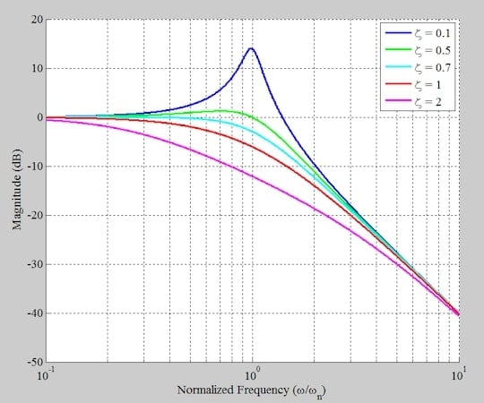
Figure 2. Magnitude response of the second-order PLL for various values of the damping factor.
When analyzing the frequency response of a second-order system, the damping factor ζ = 0.707 represents a crucial transition in the system's behavior. At ζ = 0.707, we achieve a maximally flat frequency response. In this case, the response is smooth and flat over the widest possible bandwidth before it begins to roll off.
For ζ < 0.707, the gain exhibits peaking in the frequency domain. When ζ is greater than 0.707, on the other hand, there is no gain peaking and the bandwidth of the system is narrower compared to systems with lower damping factors.
Some Insights into the Magnitude Response
The curious reader may ponder what the horizontal axis in the magnitude response of a PLL actually represents. We know that this axis represents frequency, but which parameter's frequency is it referring to?
From Equation 2, it's evident that the transfer function H(s) relates the output phase (ϕvco) to the input phase (ϕin). The magnitude response therefore characterizes the system's behavior as a function of the frequency of ϕin. Let's take a closer look at this.
When deriving the model for a PLL with a multiplier phase detector, we assumed that the input signal (vin) and the VCO output (vvco) were expressed as:
$$v_{in} ~=~ A_{in} \cos(\omega_c t~+~ \phi_{in}) \quad \text{and} \quad v_{vco} ~=~ A_{vco} \sin(\omega_c t~+~ \phi_{vco})$$
Equation 7.
If we assume that ϕin is a single-tone wave:
$$\phi_{in} ~=~ \beta \sin( \omega_m t)$$
Equation 8.
then from Equation 2, the output phase ϕvco is also a single-tone wave at ωm with an amplitude given by β × |H(jωm)|. For example, when the input phase varies slowly (ωm is small), the magnitude response is approximately equal to unity (|H(jω)| ≈ 1). Consequently, for small ωm, the output phase is equal to the input phase (ϕvco = ϕin).
As the frequency increases, the magnitude response reduces because of the circuit's lowpass behavior, leading to much smaller output phase fluctuations relative to the input. In this way, the magnitude response shows how the input phase at a given frequency ωm scales as it appears at the output.
We commonly need to have a constant scaling factor and thus avoid transfer functions with significant gain peaking. As we'll see shortly, a damping factor between 0.707 and 1 is usually employed to avoid gain peaking and provide a fast and stable response.
Closed-Loop Bandwidth
The closed-loop 3 dB bandwidth can be determined by setting the magnitude response equal to \(\frac{\sqrt{2}}{2}\) and determining the corresponding frequency. It can be shown that for ζ < 1, the 3 dB bandwidth is given by:
$$\omega_b ~=~ \omega_n \sqrt{1~-~2 \zeta^2 ~+~ \sqrt{2~-~ 4 \zeta ^2 ~+~ 4 \zeta^4}}$$
Equation 9.
For instance, with ζ = 0.1, the bandwidth works out to ωb = 1.54 × ωn. Figure 3 marks the 3 dB bandwidths for three different values of the damping factor: ζ = 0.1, 0.5, and 0.7.
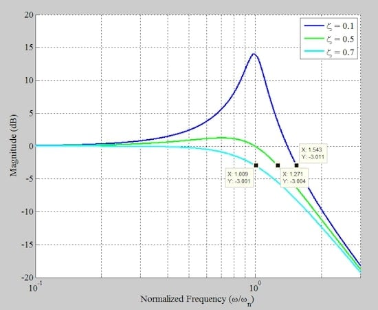
Figure 3. The closed-loop bandwidth for selected values of ζ.
Of particular interest is the case where ζ = 0.7, resulting in ωb = ωn.
Step Response
Figure 4 shows the typical step response of the second-order system described by Equation 3 for ωn = 1 rad/s and selected values of ζ.
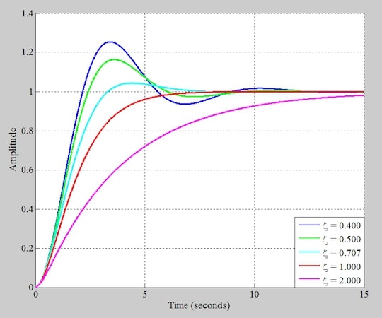
Figure 4. The step response for ωn = 1 rad/s and several values of ζ.
When examining the response in the time domain, ζ = 1 marks the point where the system's behavior transitions. For ζ < 1, we have an underdamped system, resulting in a damped sinusoidal oscillation in the output. At ζ = 1, the system is critically damped, with the transfer function having two identical poles.
For ζ > 1, the system has two distinct negative real poles. In this case, the time-domain response includes two decaying exponential terms. When ζ is considerably greater than 1, one of the two decaying exponentials reduces much more quickly than the other. Consequently, the faster-decaying exponential term (which has a smaller time constant) may be disregarded, allowing the response of the second-order system to be approximated by a simple first-order system.
Figure 4 demonstrates that an overdamped system has the slowest response. Although the figure depicts only the step response, this is true for any input. Moreover, of the systems that respond without oscillation, a critically damped system has the fastest response. A slightly underdamped system, with ζ around 0.7, gets close to the final value more rapidly than a critically damped or overdamped system.
Before we move on, note that second-order systems with closed-loop transfer functions different from Equation 3 may have step responses that differ greatly from those in Figure 4.
Step Response Rise Time
The concept of rise time is used to assess how quickly the PLL can respond to changes in the input signal. The rise time may be defined as the time it takes the output to rise from 10% to 90% of the final value. For the second-order system described by Equation 3, the rise time is commonly approximated by the following relationship:
$$t_{r} ~=~ \frac{2.2}{\omega_b}$$
Equation 10.
where ωb is the closed-loop 3 dB bandwidth.
By way of example, consider ζ = 0.7. From Equation 9, we know that ωb = ωn. If we assume that ωn = 1 rad/s, then the rise time is tr = 2.2 s. Figure 5 shows the step response for ζ = 0.7 and ωn = 1 rad/s, confirming our rise time calculation.
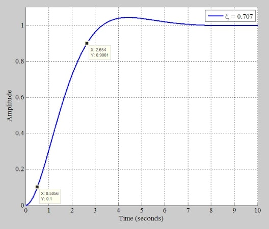
Figure 5. The step response rise time for ωn = 1 rad/s and ζ = 0.7.
Using the data points provided in the figure, the rise time is 2.654 – 0.5056 = 2.15 seconds, which is reasonably close to the calculated value.
As an aside, Equation 10 is an approximation for second-order systems like this one. However, it is exact for first-order systems.
Wrapping Up
In this article, we learned about the time- and frequency-domain behavior of the second-order Type-1 PLL, which utilizes a simple lowpass filter as its loop filter. We also examined the equations for key parameters, including the 3 dB bandwidth and rise time. In the next article, we'll assess the impact of the first-order filter on PLL performance metrics such as steady-state errors, stability, and noise performance.
This article is Part 5 of a 12-part series on loop filters in PLL design. All articles in this series are listed below in order of publication:
- Foundations for PLL Nonlinear Analysis: Modeling the Phase Detector and VCO
- Analyzing a First-Order PLL in Acquisition Mode With a Nonlinear Model
- Analyzing First-Order PLLs Using Linear Models
- Understanding the Limitations of the First-Order PLL
- Introduction to Second-Order Type-1 PLLs
- Understanding the Limitations of the Second-Order Type-1 PLL With a Lag Filter
- Analyzing the Lag Filter’s Effect on PLL Performance
- Introducing the Lag-Lead Filter
- Exploring the Bode Plots of PLLs With a Lag-Lead Loop Filter
- Understanding the Time-Domain Response of PLLs With Lag-Lead Filters
- Introduction to Second-Order Type-2 PLLs
- Second-Order Type-2 PLLs: Bode Diagrams, Bandwidth, and Overshoot
All images used courtesy of Steve Arar
Related Content