Facebook
 Google
 GitHub
 Linkedin
Analyzing the Lag Filter’s Effect on PLL Performance
In this article, we evaluate the designs of two simple frequency synthesizers to learn how a second-order PLL with a lag filter can provide a faster rise time than a first-order PLL.
So far in this article series, we have explored first-order PLLs that lack a loop filter and second-order PLLs featuring a lag filter. In this article, we'll compare these two configurations through the design of a simple frequency synthesizer using each setup. This comparative analysis will reveal both the advantages and constraints associated with the lag filter approach, paving the way for the introduction of a more complex PLL configuration in the next article.
Example 1: Synthesizer Using a First-Order PLL
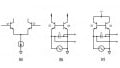
Figure 1 illustrates a frequency synthesizer that uses a first-order PLL.

Figure 1. Linearized model of a frequency synthesizer using a first-order PLL.
The signal fed back to the phase detector is the VCO output frequency (ωvco) divided by N. The frequency divider is what enables the VCO to output a frequency that is N times greater than the input frequency (ωin).
Suppose the input frequency is 10 MHz and the target output frequency is 200 MHz. If the phase detector has a gain of kd = 2 V/rad and the VCO has a gain of kvco = 2 MHz/V, calculate the loop bandwidth and the rise time.
Solution to Example 1
By substituting the frequency domain representation of the VCO's integration action (kvco/s) and applying some algebraic manipulations, we can easily derive the transfer function from ϕin to ϕvco:
$$H(s) ~=~ \frac{\phi_{vco}}{\phi_{in}} ~=~ \frac{k_d k_{vco}}{s~+~ k_d k_{vco}/N}$$
Equation 1.
Since the PLL lacks a loop filter, it operates as a first-order loop. Its transfer function is equivalent to a simple lowpass filter with a DC gain of N and a bandwidth equal to the total loop gain. The closed-loop bandwidth is therefore:
$$\omega_b ~=~ k_d k_{vco}/N$$
Equation 2.
A DC gain of N indicates that the output phase is scaled by N relative to the input phase, and the output frequency is similarly N times the input frequency. Thus, to achieve a 200 MHz output from a 10 MHz reference, a frequency division ratio of N = 20 is needed. With kd = 2 V/rad and kvco = 2 MHz/V, the bandwidth is obtained as:
$$\omega_b ~=~ k_d k_{vco}/N ~=~ (2 \ \text{V/rad}) ~\times~ (2 \pi ~\times~ 2 ~\times~ 10^6 \ \text{rad/s/V}) ~\times~ \frac{1}{20} ~=~ 0.4 \pi \ \text{Mrad/s}$$
Equation 3.
Therefore, the loop bandwidth is 0.4π ≈ 1.26 Mrad/s, or 0.2 MHz.
The first-order system's rise time, defined as the time it takes the output to rise from 10% to 90% of the final value, is given by:
$$t_{r} =~~ \frac{2.2}{\omega_b} ~=~ \frac{2.2}{4 \pi ~\times~ 10^5} ~=~ 1.75 \ \mu \text{s}$$
Equation 4.
The rise time indicates how quickly the PLL can respond to changes in the input signal.
Example 2: Synthesizer Using a Second-Order PLL
Next, let's modify the frequency synthesizer from the previous example to use a second-order PLL with a lag filter. This is shown in Figure 2.

Figure 2. A frequency synthesizer with a loop filter.
As before, assume that kd = 2 V/rad, kvco = 2 MHz/V, and N = 20. If the loop filter is given by:
$$G(s) ~=~ \frac{1}{1~+~ s / \omega_f} ~=~ \frac{\omega_f}{ s ~+~ \omega_f}$$
Equation 5.
find the value of ωf that produces a second-order, maximally flat frequency response. Then, find the closed-loop bandwidth and rise time.
Solution to Example 2
The transfer function of this PLL from ϕin to ϕvco is:
$$H(s) ~=~ \frac{\phi_{vco}}{\phi_{in}} (s) ~=~ \frac{K_0 \omega_f}{s^2 ~+~ \omega_f s ~+~ K_0 \omega_f/N}$$
Equation 6.
where K0 = kdkvco. If we express the denominator in the standard control theory form, we obtain:
$$H(s) ~=~ \frac{N \omega_n ^2}{s^2 ~+~ 2 \zeta \omega_n s ~+~ \omega_n^2}$$
Equation 7.
where ωn is the natural frequency, given by:
$$\omega_n ~=~ \sqrt{\frac{K_0 \omega_f}{N}}$$
Equation 8.
and ζ is the damping factor, given by:
$$\zeta ~=~ \frac{1}{2} \sqrt{\frac{N \omega_f}{K_0}}$$
Equation 9.
At ζ = 0.707, we achieve a maximally flat frequency response. Substituting the problem data into Equation 9, we obtain the loop filter's cutoff frequency:
$$0.707~=~\frac{1}{2} \sqrt{\frac{20 ~\times~ \omega_f}{2 ~\times~ (2 \pi ~\times~ 2 ~\times~ 10^6)}} \quad \Rightarrow \quad \omega_f ~=~ 0.8 \pi \ \text{Mrad/s}$$
Equation 10.
Next, we find the closed-loop bandwidth and rise time of the system. It can be shown that for ζ < 1, the 3 dB bandwidth of a loop with a lag filter is given by:
$$\omega_b ~=~ \omega_n \sqrt{1~-~2 \zeta^2 ~+~ \sqrt{2~-~ 4 \zeta ^2 ~+~ 4 \zeta^4}}$$
Equation 11.
For ζ = 0.707, the bandwidth works out to ωb = ωn. Applying Equation 8, we obtain:
$$\omega_b ~=~ \omega_n ~=~ \sqrt{\frac{K_0 \omega_f}{N}} ~=~ \sqrt{\frac{2 ~\times~ (2 \pi ~\times~ 2 ~\times~ 10^6) ~\times~ 0.8 \pi ~\times~ 10^6}{20}} ~\approx~ 0.56 \pi ~ \text{Mrad/s}$$
Equation 12.
Finally, the rise time of the system can be estimated by applying Equation 4, resulting in:
$$t_{r} ~=~ \frac{2.2}{\omega_b} ~=~ \frac{2.2}{0.56 \pi ~\times~ 10^6} ~=~1.25 \ \mu \text{s}$$
Equation 13.
While the first-order system's rise time is 1.75 μs, the second-order system exhibits a rise time of 1.25 μs. These rise time values are in agreement with the calculated responses of the two systems plotted in Figure 3.

Figure 3. [click to enlarge] The step response of the first-order (green) and second-order (blue) systems.
As observed, the rise time of the first-order system is 1.837 – 0.084 = 1.753 μs, and that of the second-order system is 1.494 – 0.284 = 1.21 μs.
First-Order Loop Versus PLL With Lag Filter
In order to better understand how the lag filter can improve performance relative to the first-order loop, let's repeat Example 2 for other values of ζ and compare the results with those of Example 1. To simplify the process, note that Equations 8 and 9 can be combined to express the natural frequency (ωn) in terms of ζ and the total loop gain (Kt):
$$\omega_n ~=~ 2\zeta ~\times~ K_t$$
Equation 14.
where Kt = K0/N = kdkvco/N.
Table 1 uses Equation 14 to determine ωn for ζ = 0.5, 0.707, and 0.9.
Table 1. Performance comparison between the second-order PLL with lag filter and the first-order loop.
| PLL Configuration | ωn (rad/s) | ωb (rad/s) | Rise Time (μs) |
| Second-Order (ζ = 0.5) | Kt | 1.27 × Kt | 1.38 |
| Second-Order (ζ = 0.707) | 1.41 × Kt | 1.41 × Kt | 1.24 |
| Second-Order (ζ = 0.9) | 1.8 × Kt | 1.34 × Kt | 1.31 |
| First-Order Loop | NA | Kt | 1.75 |
The third column of the table uses Equation 11 to determine the closed-loop bandwidth (ωb) for different values of ζ. While the bandwidth of the first-order system (Equation 3) is equal to the total loop gain, the bandwidth of the second-order system is wider by a factor between 1.27 and 1.41, contingent on the selected ζ value. As a result, the second-order system provides a faster rise time for a given loop gain.
Another advantage is that the loop filter removes undesirable components from the phase detector and provides further control over the loop's frequency response.
However, the performance enhancement provided by this simple loop filter is relatively constrained. It introduces just one additional design parameter: the loop filter's cutoff frequency (ωf), which is fully determined by ζ and loop gain (see Equation 9). Furthermore, because of the trade-off between stability and loop gain, there is a maximum allowable loop gain for a given value of ζ.
This means that we haven't made substantial progress in improving loop performance or in independently selecting the loop parameters. For example, we cannot choose the loop gain and bandwidth independently. In the next article, we'll start investigating how more complicated filters can influence performance and enhance our control over the loop properties.
This article is Part 7 of a 12-part series on loop filters in PLL design. All articles in this series are listed below in order of publication:
- Foundations for PLL Nonlinear Analysis: Modeling the Phase Detector and VCO
- Analyzing a First-Order PLL in Acquisition Mode With a Nonlinear Model
- Analyzing First-Order PLLs Using Linear Models
- Understanding the Limitations of the First-Order PLL
- Introduction to Second-Order Type-1 PLLs
- Understanding the Limitations of the Second-Order Type-1 PLL With a Lag Filter
- Analyzing the Lag Filter’s Effect on PLL Performance
- Introducing the Lag-Lead Filter
- Exploring the Bode Plots of PLLs With a Lag-Lead Loop Filter
- Understanding the Time-Domain Response of PLLs With Lag-Lead Filters
- Introduction to Second-Order Type-2 PLLs
- Second-Order Type-2 PLLs: Bode Diagrams, Bandwidth, and Overshoot
All images used courtesy of Steve Arar