 Facebook
 Google
 GitHub
 Linkedin
Analyzing the Moog Filter
Learn about one of the only audio filter topologies out there, the Moog filter!
Learn about one of the only audio filter topologies out there, the Moog filter!
Of the voltage-controlled audio filter topologies, there are few. This piques my interest in such a circuit—clearly, a voltage-controlled filter (VCF) is a useful, maybe even an essential, element in audio circuits!
And with all the creativity of 20th-century analog engineers, the fact that these circuits are scarce is fascinating. Why are there so few topologies? Why don't any of the existing topologies look much like filters?
Voltage-Controlled Filters for Audio Applications
Voltage-controlled filters (or VCFs) were a mainstay of the analog synthesizer. The most common configuration, arguably, uses the operational transconductance amplifier (OTA) based filter, with such ICs as the LM13600 and the LM3080 being popular choices. Korg had manufactured chips such as the Korg35, based on either a clever Sallen-Key arrangement or an OTA, depending on the time of manufacture, and ARP manufactured the 4023, 4035, and 4075 modules, which utilized an OTA, a Moog topology, and a current-feedback op-amp, respectively.
But one filter stands above the rest, for being creative, effective, and (I have on good authority) audibly "brilliant". This is the Moog ladder filter.
The Moog Ladder Filter Schematic
Without further ado, let's take a look at the Moog filter, roughly as it appeared in the Moog Prodigy.
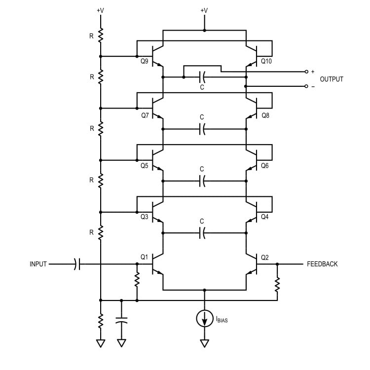
Figure 1. The famous Moog filter, as it appeared in the Moog Prodigy analog synthesizer.
We see here eight transistors in a "ladder", biased with a resistive divider chain, being driven by a bias/control current Ibias. Audio input is applied to Q1, feedback (for resonance, also known as emphasis in electronic music) is applied to Q2, and the other transistors are in pairs, tied at the base, with capacitors shunting their emitters. The output is taken as the voltage across the top-most capacitor. To simplify this a little bit, we can (with some care) remove the biasing components, and we get the schematic shown in Figure 2.
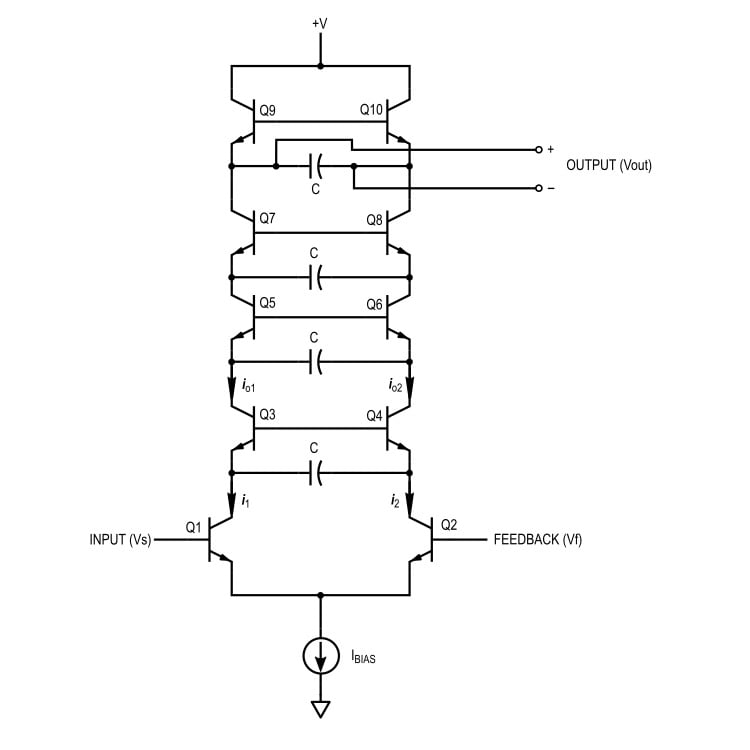
Figure 2. Simplified schematic of the Moog filter
This is only slightly misleading, because of course the bases are not floating, but are held at constant potential through a divider.
The Moog Ladder Filter Explained
Let's just look at the circuit. The cutoff-frequency control for the circuit is a current, Ibias, applied to a differential pair Q1-Q2. Changing Ibias causes the bias current of the transistors to change, for the whole network. Neglecting base currents (i.e., assuming high beta) we see that whatever DC current flows through Q1 must flow through the rest of the left-side ladder, and similarly for Q2 and the right-side.
The transistor pairs Q3-Q4, Q5-Q6, and Q7-Q8 each have two transistors and a capacitor. The transistors in a pair share the same base voltage but have different emitter currents. Because the small-signal currents are different, the small-signal vbe for the transistors will be different, and so a potential will develop across the emitter capacitor. The capacitor, being a frequency-dependent reactance, gives rise to the filtering effect.
That's the idea anyway. To see how accurate this is, we must analyze the three distinct parts of the filter, shown in Figure 3.
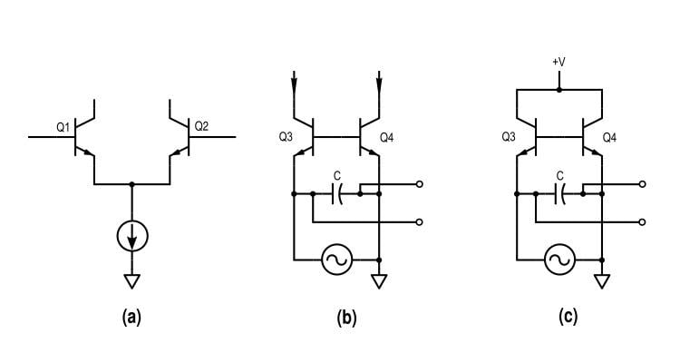
Figure 3. The three elements of the ladder filter topology. (a) The driving differential pair. (b) A mid-ladder low-pass filter section. (c) The top-most output filter section.
The circuit can be broken up into a driver (Figure 3a) and low-pass filters (Figure 3b and 3c). The input sources to (b) and (c) are current signals, grounded on the feedback side for ease of analysis (the reader can confirm that this is safe by symmetry).
Driver
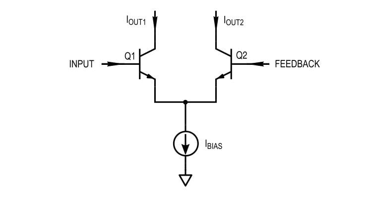
Figure 4. The driving section of the filter.
The driving section is a differential pair, also known as an emitter-coupled pair. To analyze this circuit from a small-signal perspective, we can replace the transistors with appropriate audio-frequency active-region models. Two common choices are the hybrid-pi model (transconductance modeled with an input resistance) or the T model (transconductance modeled with a base-emitter resistance).
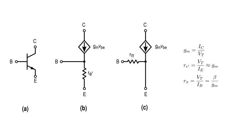
Figure 5. Three transistor models. (a) An NPN transistor. (b) The T model. (c) The hybrid-pi model.
The resistances in the T model and hybrid-pi model are related by a factor equal to the transistor beta. Though they have different circuit configurations, the models are analytically identical. For the driver circuit, we can use the hybrid-pi model.
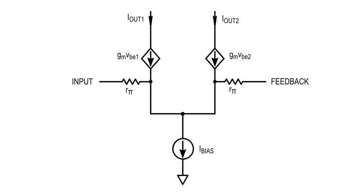
Figure 6. We can model the transistors in the driver with the transistors' low-frequency hybrid-pi equivalent.
The circuit can be simplified by replacing constant current sources with open circuits and constant voltage sources with ground connections, as shown in Figure 7. For small-signal current gain calculations, the loads are shorted, allowing us to effectively ground the collectors as well.
Normally, we would also be calculating the output impedance to account for loading, but in this case, we won’t have to. This can be justified by the presence of the dependent current sources, and because we are not considering the Early effect (which would appear as an output impedance in parallel with the current sources). We will not consider common-mode effects, because the bias point of the transistors is sufficiently small.
Finally, to model the differential input, we’re going to apply equal and opposite input voltages to both transistors. This isn’t strictly necessary, but it will make analysis easier.
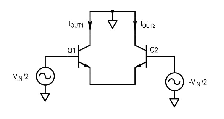
Figure 7. Small-signal circuit for analysis, using a few simplification techniques.
Something that may not be obvious here is the fact that the transistor emitters are going to be at a fixed potential (AC ground). This is due to the symmetry of the circuit.
Essentially, any AC current driven by Q1 is going to pass through Q2, and the pi-model base resistors will not have any of that dependent current passing through them. No voltage change occurs, and so we can safely ground the emitters.
This gives us the circuit shown in Figure 8 (a). Note that because of the grounding, the two halves of the circuit can be analyzed separately, as shown with the transistor pi-model in (b).
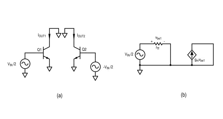
Figure 8. (a) the final small-signal circuit for analysis, (b) one side of the differential circuit, a ‘half circuit.’
The driving current is given by
$$I_{OUT1} = -I_{OUT2} = g_m v_{be1} = \frac{g_m v_{in}}{2}$$
Where vin is the total differential small-signal voltage input to the driving stage. In the absence of feedback, this is equal to the filter input.
In summary, the driver section is made up of a differential pair of transistors, which provide the differential input current to the ladder. This input current depends on gm, and therefore on the transistors' bias currents and temperature.
Conclusion
In the first part of this series on the Moog ladder filter topology, we looked at the topology as a whole, expressed our assumptions, and began our analysis with the driver section.
In the upcoming articles, we will analyze the filter sections of the Moog filter, and then, using all of our results, we will describe the open-loop transfer characteristics of the topology as a whole.


Man, I love this piece. Thanks for writing it. I once developed a DSP-based Moog emulator written on a Motorola DSP56k DSP. I couldn’t get it sounding convincing enough for people who knew what they were listening for, but in the end it was a nice digital effect. Can’t wait for the upcoming articles to learn more about the analog design principles behind this iconic sound. Way to go.
“The transistors in a pair share the same base voltage but have different emitter currents.”
Can you help me understand why they have different emitter currents please?