Facebook
 Google
 GitHub
 Linkedin
Analyzing First-Order PLLs Using Linear Models
In this article, we'll use the linearized model of a first-order PLL to understand its response to a simple input change. We'll then use Matlab simulations to visualize the signals.
As we learned in the previous article, an analog PLL is generally a nonlinear system because its phase detector exhibits a nonlinear sinusoidal characteristic. However, when the loop is locked and the phase error is small, the PLL can be represented by a linear time-invariant (LTI) model. Because it allows us to use control theory concepts such as the Laplace transform to analyze the loop behavior, this is a significant advantage.
In this article, we'll embark on our journey of PLL design by exploring the linearized model of the simplest PLL configuration: the first-order PLL. Using the linearized model, we'll examine the loop behavior in response to inputs such a phase step. In the next article, we'll discuss the PLL's response to a frequency step and frequency ramp.
Nonlinear Model of a PLL
Figure 1 shows the basic block diagram of a PLL with a multiplier phase detector.
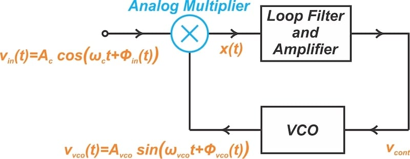
Figure 1. Basic block diagram of a PLL.
Substituting the multiplier and VCO with their respective models results in the nonlinear PLL model depicted in Figure 2.
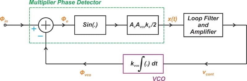
Figure 2. Nonlinear model of a PLL with a multiplier phase detector.
In the above figure, ϕin is the input phase and ϕvco is the output phase. An important signal in this system is the phase error (ϕe), defined as:
$$\phi_{e}(t) ~=~ \phi_{in}(t) ~-~ \phi_{vco}(t)$$
Equation 1.
The sine function in this model introduces nonlinearity, complicating the system analysis. When the PLL locks, however, it tracks the input signal. This means the phase difference between the VCO output and the input signal is minimized, ideally to zero or a small constant value.
The PLL maintains this state of synchronization by continuously adjusting the VCO in response to any changes in the input signal. Given the small phase error, we can approximate the sine function with its linearized equivalent model.
The Linearized PLL Model
If we assume that the phase error is sufficiently small, we can approximate the sine function as follows:
$$\sin( \phi_e) ~\approx~ \phi_e$$
Equation 2.
This allows us to model the PLL with an LTI system when it's locked. The linearized model of the analog PLL is shown in Figure 3.
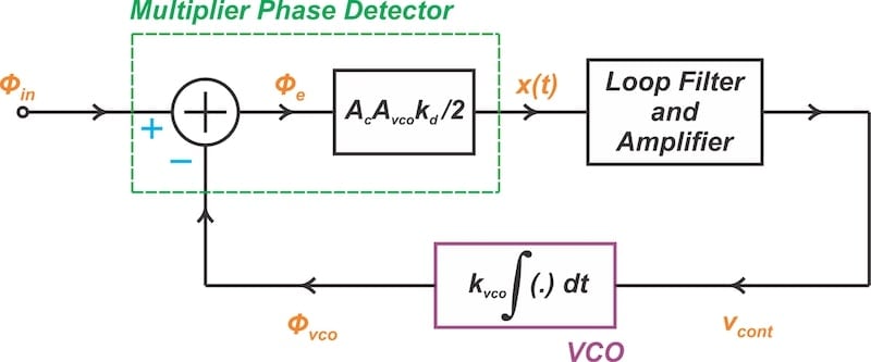
Figure 3. Linear model of a PLL with a multiplier phase detector.
The VCO's transfer function in the frequency domain is:
$$\frac{\phi_{vco}}{v_{cont}}(s) ~=~ \frac{k_{vco}}{s}$$
Equation 3.
where s = jω is the complex frequency (Laplace) variable. Therefore, the frequency-domain model of the PLL is as illustrated in Figure 4.
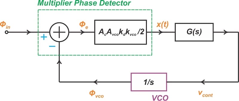
Figure 4. Linear model of the PLL in the frequency domain.
When analyzing a PLL's linear model, it's useful to look at two different transfer functions. The first transfer function, H(s), describes the relationship between ϕin to ϕvco. Using some algebra, H(s) is obtained as:
$$H(s) ~=~ \frac{\phi_{vco}}{\phi_{in}} (s) ~=~ \frac{K_0 G(s)}{s~+~K_0 G(s)}$$
Equation 4.
where G(s) is the loop filter's transfer function and K0 is the total loop gain. Note that in the above figures, K0 is expressed as 0.5AcAvcokdkvco.
The second transfer function, He(s), gives the relationship between the input phase (ϕin) and the phase error (ϕe):
$$H_e(s)~=~\frac{\phi_e}{\phi_{in}} (s) ~=~ \frac{\phi_{in}~-~\phi_{vco}}{\phi_{in}}~=~ 1~-~H(s) ~=~ \frac{s}{s~+~K_0 G(s)}$$
Equation 5.
By examining H(s) and He(s), we can determine how the PLL tracks different types of inputs and identify the feedback loop error as it attempts to do so.
The First-Order PLL
The most basic PLL is formed by setting G(s) = 1, implying that no lowpass filter is utilized. This results in the following transfer functions:
$$H(s) ~=~ \frac{\phi_{vco}}{\phi_{in}} (s) ~=~ \frac{K_0}{s~+~K_0}$$
Equation 6.
and:
$$H_e(s)~=~\frac{\phi_e}{\phi_{in}}(s) ~=~ \frac{s}{s~+~K_0}$$
Equation 7.
Note that if the loop gain is positive (K0 > 0), the system has a single pole at s = –K0. It is therefore stable. Also, H(s) is equivalent to a lowpass filter with DC gain of unity and –3 dB bandwidth of K0.
This PLL is referred to as a first-order loop because it can be described by a first-order differential equation. In the next section, we'll see how the loop responds to a phase step.
First-Order PLL Tracking a Phase Step
When a step change of magnitude Δϕ occurs in the input phase, we have:
$$\phi_{in}(t)~=~ \Delta \phi \ u(t) \xrightarrow{\text{Laplace}} \phi_{in}(s) ~=~ \frac{\Delta \phi}{s}$$
Equation 8.
where u(t) is the unit step function. Substituting ϕin(s) into Equation 6 yields the output phase as:
$$\phi_{vco}(s) ~=~ \frac{K_0}{s~+~K_0} ~\times~ \phi_{in} (s) ~=~ \frac{K_0}{s~+~K_0} ~\times~ \frac{\Delta \phi}{s}$$
Equation 9.
Applying a partial fraction expansion, the above equation can be rewritten as:
$$\phi_{vco}(s) ~=~ \frac{\Delta \phi}{s} ~-~ \frac{\Delta \phi}{s~+~K_0}$$
Equation 10.
Taking the inverse Laplace transform yields the output phase in the time domain:
$$\phi_{vco}(t) ~=~ \Delta \phi \big (1 ~-~ e^{-K_0t} \big ) \ u(t)$$
Equation 11.
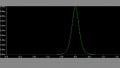
Figure 5 plots ϕin(t) and ϕvco(t) for Δϕ = 1 and K0 = 400π rad/s.
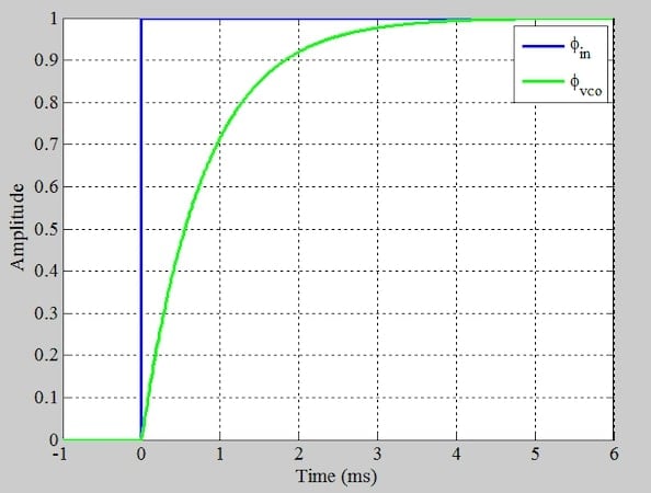
Figure 5. Response of a first-order PLL to a phase step.
After the transients go to zero, the output phase equals the input phase. The first-order PLL can track a sudden change in the input phase with zero steady-state phase error (ϕe = 0).
Simulating the PLL Response to a Phase Step
Using Matlab, I've simulated the first-order PLL model shown in Figure 3 with the following parameters:
- Ac = Avco = 1 V
- kd =4 V-1
- kvco = 400π rad/sV
- A VCO free-running frequency of 4 kHz.
To enhance our understanding, let's examine its simulated response to a step change in the input phase. As illustrated in Figure 6, the input waveform features a 4 kHz signal with a phase step of π/2 occurring at t = 2 ms.
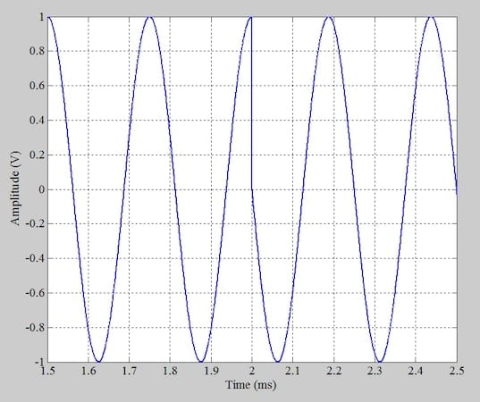
Figure 6. Input signal applied to the PLL.
Figure 7 illustrates the VCO control voltage as the PLL reacts to the phase step at the input.
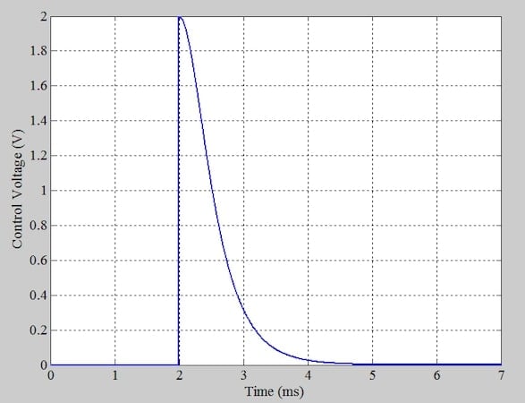
Figure 7. The control voltage waveform while the PLL tracks the input phase.
The VCO frequency is solely influenced by the control voltage. As we observe in Figure 7, the control voltage starts at 0 V, experiences some changes, and finally settles back to 0 V.
The initial and final values of the control voltage are zero because the input signal matches the VCO's free-running frequency. However, upon detecting a phase difference, the feedback loop adjusts the VCO frequency, allowing it to either speed up or slow down phase accumulation to eventually synchronize with the input signal's phase.
The PLL input and VCO output signals are shown in Figure 8, along with some data points to help us verify the loop behavior. Note that the points may be hard to read in the image below. Clicking on the figure will open a larger, more legible version.
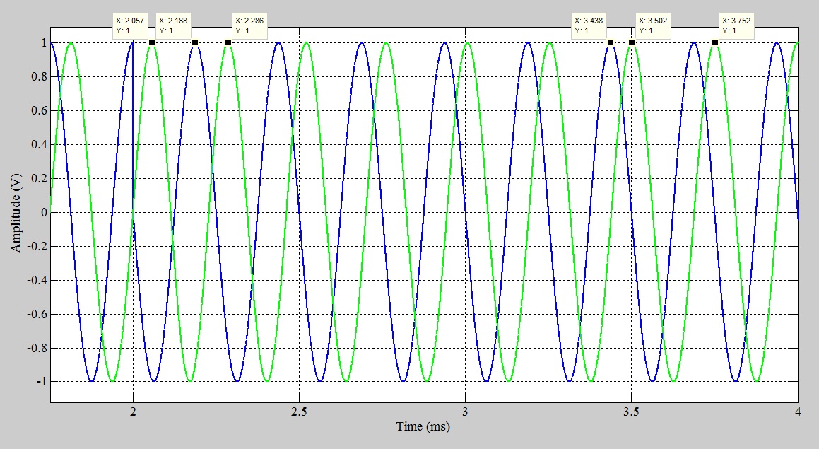
Figure 8. [click to enlarge] Comparing the waveforms of the PLL input (blue) and the VCO output (green).
From the data points associated with the VCO's peaks at times t = 2.057 ms and 2.286 ms, we see that the VCO frequency is nearly 4.37 kHz after the phase step. On the other hand, the data points associated with times t = 3.502 ms and 3.752 ms show that the VCO frequency reduces to 4 kHz just before t = 4 ms. As shown in Figure 7, the control voltage drops back to nearly zero at t = 4 ms.
Additionally, note how the phase difference between the input signal and VCO output changes over time. Before applying the phase step at t = 2 ms, there's a phase difference of 90 degrees between the two waveforms. The peak of the blue waveform occurs when the rising part of the green waveform crosses zero. This 90-degree phase difference results from using a multiplier phase detector.
Directly after the phase step, the phase difference exceeds 90 degrees. Using the data points provided in Figure 8, the time difference between the peaks of the two waveforms is 2.188 – 2.057 = 0.131 ms. If we assume that the two signals are at 4 kHz, which corresponds to a period of 0.25 ms, a time difference of 0.131 ms corresponds to a phase difference of about 188.6 degrees.
However, the loop then tries to follow the input phase, bringing the phase difference back to 90 degrees at about t = 4 ms. This confirms that the first-order PLL can track a phase step with zero steady-state error.
Wrapping Up
While PLLs are generally nonlinear systems, we can model them as LTI systems when the loop is locked and the phase error is small. This allows us to use control theory concepts, such as the Laplace transform, to analyze the loop behavior. In this article, we analyzed the linearized model of the simplest PLL configuration, the first-order PLL, in response to a phase step.
We found that the first-order PLL eventually adapts to any step change in the input phase. In future articles, we'll continue our discussion of PLLs by exploring these key questions:
- How does the first-order PLL react to more complex inputs, like a frequency step or a frequency ramp?
- How would incorporating a loop filter alter the response?
This article is Part 3 of a 12-part series on loop filters in PLL design. All articles in this series are listed below in order of publication:
- Foundations for PLL Nonlinear Analysis: Modeling the Phase Detector and VCO
- Analyzing a First-Order PLL in Acquisition Mode With a Nonlinear Model
- Analyzing First-Order PLLs Using Linear Models
- Understanding the Limitations of the First-Order PLL
- Introduction to Second-Order Type-1 PLLs
- Understanding the Limitations of the Second-Order Type-1 PLL With a Lag Filter
- Analyzing the Lag Filter’s Effect on PLL Performance
- Introducing the Lag-Lead Filter
- Exploring the Bode Plots of PLLs With a Lag-Lead Loop Filter
- Understanding the Time-Domain Response of PLLs With Lag-Lead Filters
- Introduction to Second-Order Type-2 PLLs
- Second-Order Type-2 PLLs: Bode Diagrams, Bandwidth, and Overshoot
All images used courtesy of Steve Arar