Facebook
 Google
 GitHub
 Linkedin
Understanding the Limitations of the First-Order PLL
Higher-order PLLs are more commonly used than first-order PLLs. To explain why, we explore the first-order PLL's behavior in response to two inputs: a frequency step and frequency ramp.
The previous article in this series explored the linear model of the first-order PLL. We found that the first-order PLL tracks a step change in input phase with zero steady-state error. In this article, we'll continue our discussion by exploring the first-order PLL's behavior in response to more complex inputs, namely a frequency step and a frequency ramp. The exploration will reveal key limitations of the first-order PLL, explaining why it's rarely used in practice.
The First-Order PLL: A Review
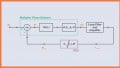
Figure 1 shows the basic block diagram of a PLL with a multiplier phase detector.
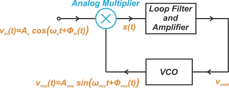
Figure 1. Basic block diagram of a PLL.
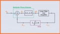
By linearizing the above model and opting not to use a loop filter, we derive the first-order PLL's linear model (Figure 2).
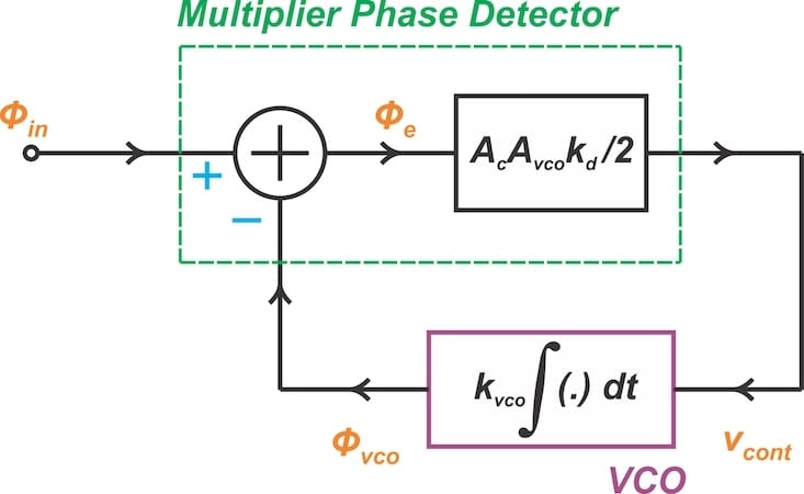
Figure 2. The linearized model of a first-order PLL with a multiplier phase detector.
In this model, the overall loop gain (K0) is defined as:
$$K_0~=~ \frac{1}{2}A_cA_{vco}k_dk_{vco}$$
Equation 1.
where:
Ac is the input amplitude
Avco is the VCO output amplitude
kd is the multiplier's gain factor in V-1
kvco is the VCO gain factor measured in rad/sV.
Note that K0 is expressed in terms of rad/s.
To understand the system behavior, we examine two different transfer functions. The first of these, H(s), describes the relationship between the input phase (ϕin) and the output phase (ϕvco):
$$H(s) ~=~ \frac{\phi_{vco}}{\phi_{in}} (s) ~=~ \frac{K_0}{s~+~K_0}$$
Equation 2.
The second transfer function, He(s), gives the relationship between ϕin and the phase error (ϕe):
$$H_e(s)~=~\frac{\phi_e}{\phi_{in}} (s) ~=~ \frac{s}{s~+~K_0}$$
Equation 3.
First-Order PLL Tracking a Frequency Step
A step change in the PLL's input frequency is a common practical scenario, which is why it's widely used to evaluate PLL performance. In practice, a frequency step is often encountered when the PLL is first powered on. This is because the PLL's incoming frequency rarely matches the VCO's free-running frequency exactly.
Another typical example would be when a transmitter and receiver synchronized to the same frequency start to move relative to each other. This results in a Doppler shift, creating a frequency offset.
But how can we analyze the PLL behavior in response to a frequency step? You can easily verify that when there is a step change in frequency, the input phase varies as a ramp function. Assume that for t > 0, the input phase increases at a constant rate of 2πΔf radians per second. Therefore, the input phase may be expressed as:
$$\phi_{in}(t) ~=~ (2 \pi \Delta f ~\times~ t) \ u(t)$$
Equation 4.
where u(t) is the unit step function. The Laplace transform of ϕin(t) is:
$$\phi_{in}(s) ~=~ \frac{2 \pi \Delta f}{s^2}$$
Equation 5.
Combining the above equation with Equation 3, we determine the phase error in the frequency domain:
$$\phi_e(s) ~=~ \frac{s}{s~+~K_0} \phi_{in}(s) ~=~ \frac{s}{s~+~K_0} ~\times~ \frac{2 \pi \Delta f}{s^2}$$
Equation 6.
Applying a partial fraction expansion, we can rewrite the above equation as:
$$\phi_e(s) ~=~ \frac{2 \pi \Delta f}{K_0} \big (\frac{1}{s} ~-~ \frac{1}{s~+~K_0} \big )$$
Equation 7.
Taking the inverse Laplace transform, the time domain expression is obtained as:
$$\phi_e(t) ~=~ \frac{2 \pi \Delta f}{K_0} \big (1 ~-~ e^{-K_0 t} \big ) u(t)$$
Equation 8.
At t = ∞, the phase error (ϕe) works out to:
$$\phi_e(t~=~\infty) ~=~ \frac{2 \pi \Delta f}{K_0}$$
Equation 9.
The steady-state error has a constant non-zero value. This shows that the loop locks to the input frequency, and the VCO frequency is the same as the input frequency. However, there's a static phase error between the input and the VCO output even after locking has taken place.
Note that the steady-state phase error is inversely proportional to the loop gain (K0). From Equation 2, we observe that H(s) is equivalent to a lowpass filter with –3 dB bandwidth of K0. This means that the closed-loop bandwidth is also determined by K0. Increasing the loop gain therefore reduces the tracking phase error (Equation 9) while increasing the loop bandwidth.
Although this larger bandwidth allows for a faster loop response, it also makes the PLL less effective at filtering noise. This is a key reason why the first-order PLL is seldom used in practical applications.
Before we move on, take note that while the phase error is non-zero, the steady-state frequency error in response to a frequency step is zero. In other words, the VCO frequency is the same as the input frequency.
Simulating the PLL Response to a Frequency Step
In the previous article, we simulated the first-order PLL's response to a phase step. Now, we'll use the same method to examine its response to a step change in input frequency. I used Matlab to simulate the PLL model shown in Figure 2 with the following parameters:
- Ac = Avco = 1 V
- kd = 4 V-1
- kvco = 400π rad/sV
- VCO free-running frequency of 4 kHz.
As illustrated in Figure 3, the input frequency begins at 4 kHz and jumps to 4.1 kHz at t = 2 ms. This relatively small frequency step was selected to ensure the linear model of the PLL maintains sufficient accuracy.
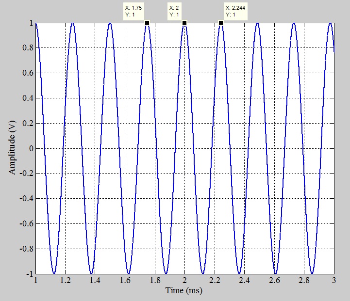
Figure 3. [click to enlarge] Input signal applied to the PLL.
The data points in the figure above can be used to verify the frequency before and after t = 2 ms. Figure 4 shows the VCO control voltage as the PLL responds to the frequency step at the input.
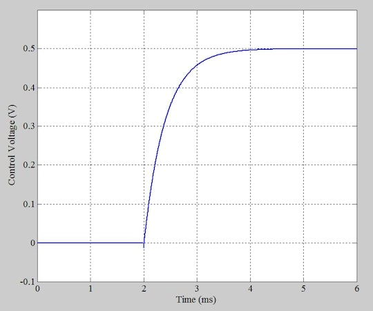
Figure 4. The control voltage waveform while the PLL tracks the frequency step.
At the start, the input frequency matches the VCO's free-running frequency, so the control voltage is at 0 V. Upon a positive frequency step at t = 2 ms, the feedback loop boosts the VCO's control voltage to adjust its frequency to match the input frequency. The final voltage change in the control voltage is 0.5 V. Multiplying 0.5 V by the VCO's gain factor of kvco = 400π rad/sV, we obtain the variation in the VCO's frequency:
$$\Delta \omega_{vco} ~=~ 0.5 ~\times~ 400 \pi ~=~ 200 \pi \; \text{rad/s}$$
Equation 10.
This corresponds to a frequency variation of 100 Hz at the VCO output, which is consistent with the applied frequency step. The input waveform and the VCO's output waveform are shown together in Figure 5.

Figure 5. [click to enlarge] Comparing the waveforms of the PLL input (blue) and the VCO output (green).
Note how the phase difference between the two signals changes over time. Before applying the phase step at t = 2 ms, the time difference between the peaks of the two waveforms is 1.813 – 1.751 = 0.062 ms. At a frequency of 4 kHz, this time difference corresponds to a phase difference of about 90 degrees. This 90-degree phase difference results from using a multiplier phase detector.
Following the application of the frequency step, the phase difference between the two signals changes during the transient response of the system. After the transients die out, the time difference between the peaks of the two waveforms is 5.486 – 5.415 = 0.071 ms. At a frequency of 4.1 kHz, this time difference corresponds to a phase difference of about 104.8 degrees.
Subtracting the nominal 90-degree phase difference caused by the multiplier phase detector, the phase error between the two signals is 14.8 degrees. Let's compare this with the phase error predicted by Equation 9. The total loop gain in our example is:
$$K_0~=~0.5A_c A_{vco} k_d k_{vco}~=~0.5 ~\times~ 1 ~\times~ 1 ~\times~ 4 ~\times~ 400 \pi~=~800 \pi \ \text{rad/s}$$
Equation 11.
With a frequency step of Δf = 100 Hz, Equation 9 yields the phase error as:
$$\phi_e(t~=~\infty) ~=~ \frac{2 \pi \Delta f}{K_0} ~=~ \frac{2 \pi ~\times~ 100}{800 \pi} ~=~ 0.25 \ \text{rad} =~~ 14.32 \ \text{degrees}$$
Equation 12.
which is consistent with the simulation result.
Applying a Frequency Ramp to a First-Order PLL
Another test input of interest is a frequency ramp, where the input frequency changes linearly over time. In the real world, you might encounter a frequency ramp when a transmitter and receiver are moving relative to each other with constant acceleration. In this case, the Doppler effect induces a carrier frequency change resembling a ramp function.
Another situation where a frequency ramp is observed is sweep-frequency modulation. This technique, which finds use in radar systems, varies the frequency of the carrier signal continuously over a range of frequencies.
Assume that the input frequency changes at a rate of R Hz/s, or equivalently the input frequency is fin(t) = Rt × u(t) Hz. Since phase is the integral of frequency, the input phase is obtained as:
$$\phi_{in}(t) ~=~ 2 \pi \int_0 ^t Rt \ dt ~=~ \pi R t ^2 \ u(t)$$
Equation 13.
Taking the Laplace transform of the above equation produces:
$$\phi_{in}(s) ~=~ \frac{2 \pi R}{s^3}$$
Equation 14.
Substituting ϕin(s) from the above equation into Equation 3, we can find the phase error in response to a frequency ramp:
$$\phi_e(s) ~=~ \frac{s}{s~+~K_0} \phi_{in}(s) ~=~ \frac{s}{s~+~K_0} ~\times~ \frac{2 \pi R}{s^3}$$
Equation 15.
Applying a partial fraction expansion, we can rewrite the above equation as:
$$\phi_e(s) ~=~ \frac{2 \pi R}{K_0} \Big ( -\frac{1}{K_0 s} ~+~ \frac{1}{s^2} ~+~ \frac{1}{K_0 (s~+~K_0)} \Big )$$
Equation 16.
Finally, taking the inverse Laplace transform, the phase error in the time domain is obtained:
$$\phi_{e}(t) ~=~ \frac{2 \pi R}{K_0} \big ( -\frac{1}{K_0} ~+~ t ~+~ \frac{1}{K_0}e^{-K_0 t} \big) \ u(t)$$
Equation 17.
The error in response to a frequency ramp increases with time without bound. In practice, the error will grow until the linear bounds are eventually passed, making our assumption of dealing with an LTI system invalid. For that reason, a first-order PLL is not suitable for tracking a frequency ramp.
Final-Value Theorem
Previously, we determined the PLL's steady-state error by calculating the phase error in the time domain, ϕin(t). Another approach to finding the steady-state error is to use the final-value theorem. According to this theorem, if x(t) is a time-domain function and X(s) is its Laplace transform, then the final value of x(t) as t tends to infinity can be found using the following formula:
$$\lim_{t \to \infty} x(t) ~=~ \lim_{s \to 0} sX(s)$$
Equation 18.
The final-value theorem allows us to determine the steady-state value of a function in the time domain from its Laplace transform, which is in the frequency domain. As an example, let's apply this method to calculate the first-order PLL's error in response to a frequency step. Substituting the phase error, ϕe(s), from Equation 6 into Equation 18, we obtain:
$$\lim_{t \to \infty} \ {\phi (t)} ~=~ \lim_{s \to 0} \ s{\phi_e}(s) ~=~ \lim_{s \to 0} \ s ~\times~ \frac{s}{s~+~K_0} ~\times~ \frac{2 \pi \Delta f}{s^2} ~=~ \frac{2 \pi \Delta f}{K_0}$$
Equation 19.
which is consistent with our time-domain analysis.
Wrapping Up
A first-order PLL adjusts to any step change in the input phase. Though it will also track a step change in input frequency, this produces a phase error. This phase error will be proportional to the magnitude of the frequency step and inversely proportional to the DC loop gain. For a frequency ramp, the phase error increases continuously over time.
Table 1 provides a summary of the first-order PLL's steady-state phase error for the inputs described above.
Table 1. The first-order PLL's phase error in response to various inputs.
|
|
Phase Step (Δϕ)
rad |
Frequency Step (Δf)
Hz |
Frequency Ramp (R)
Hz/s |
| First-Order PLL Phase Error | 0 | 2πΔf/K0 | ∞ |
A high DC loop gain is beneficial for minimizing steady-state error. In a first-order PLL, however, it results in increased bandwidth. Although this larger bandwidth allows for a faster loop response, it also makes the PLL less effective at filtering noise.
As a result of these limitations, the first-order PLL is seldom used in practice. In future articles, we'll learn about more complex PLLs that try to address these limitations.
This article is Part 4 of a 12-part series on loop filters in PLL design. All articles in this series are listed below in order of publication:
- Foundations for PLL Nonlinear Analysis: Modeling the Phase Detector and VCO
- Analyzing a First-Order PLL in Acquisition Mode With a Nonlinear Model
- Analyzing First-Order PLLs Using Linear Models
- Understanding the Limitations of the First-Order PLL
- Introduction to Second-Order Type-1 PLLs
- Understanding the Limitations of the Second-Order Type-1 PLL With a Lag Filter
- Analyzing the Lag Filter’s Effect on PLL Performance
- Introducing the Lag-Lead Filter
- Exploring the Bode Plots of PLLs With a Lag-Lead Loop Filter
- Understanding the Time-Domain Response of PLLs With Lag-Lead Filters
- Introduction to Second-Order Type-2 PLLs
- Second-Order Type-2 PLLs: Bode Diagrams, Bandwidth, and Overshoot
All images used courtesy of Steve Arar