Facebook
 Google
 GitHub
 Linkedin
Nanoscale SCE: Electrostatic Challenges and FinFET/GAA Mitigation Solutions
Learn how scaling beyond Dennard's limits triggered short-channel effects (SCE) and why transitioning from FinFET to Gate-All-Around (GAA) architectures is vital for 2 nm control.
Moore’s Law has driven MOS from micrometer-scale toward the atomic regime. While Dennard’s scaling provided a framework for proportional gains in switching speed and power efficiency, its validity declined in the deep-submicron era due to fundamental physical constraints. For example, Short Channel Effects (SCE) undermine gate control, increase leakage, and disrupt predictable switching behavior.
New architectures, such as FinFETs, Gate-All-Around (GAA), and 2D-material transistors, are designed to provide better control over current flow as devices shrink to nanometer scales. But this added complexity to manufacturing and design. This article explains practical, layout-oriented strategies engineers can use to bring back control and keep leakage in check at advanced nodes.
The Breakdown of Dennard Scaling: Physical Limits in the Deep Sub-Micron technology
Dennard’s Scaling theory postulated that the internal electric fields would remain constant if the channel length, width, oxide thickness, and the supply voltage were lowered by a factor k, while increasing the substrate doping by the same factor. This 'constant field’ established a scaling trajectory: power density remained invariant, while switching speed, drive current, and transistor density improved generation after generation [1]. This relationship became the engine behind the industry’s exponential progress, enabling the doubling of transistor density famously predicted by Moore.
In the deep sub-micron era (below 0.25 um), physical limits increasingly constrained further reductions in threshold voltage and gate-oxide thickness. Lowering the threshold voltage caused massive leakage current, while making the oxide thickness thinner than 1.5 nm made electrons tunnel straight through the gate. So, the supply voltage could not be reduced enough, causing dangerously high electric fields.
When the channel length became comparable to the source and drain depletion regions, the old rules failed, and scaling trends indicate that deep-nanometer devices face increasingly severe electrostatic constraints [2]. Figure 1 describes the microprocessor scaling trends, illustrating the breakdown of Dennard scaling and its impact on performance, frequency, and power consumption.
![Figure 1. Microprocessor scaling trends [2].](https://www.allaboutcircuits.com/uploads/articles/Si-Vision_Nanoscale_Fig_1.jpg)
Figure 1. Microprocessor scaling trends [2].
The Phenomenology of SCEs
In an ideal long-channel MOSFET, the Vds serves only to sweep carriers across the channel once they have surmounted this barrier. In a short-channel device, however, the proximity of the drain to the source allows the drain’s electric field to penetrate the channel and directly influence the source potential barrier. This 2D electrostatic coupling is the root cause of SCEs.
Drain-Induced Barrier Lowering (DIBL)
As the drain voltage increases, the depletion region associated with the drain-body junction expands. In short-channel devices, this depletion region extends far enough to interact with the source depletion region, lowering the potential barrier and hence the gate controllability, as shown in Figure 2.
![Figure 2. Energy Band Diagram of DIBL [3].](https://www.allaboutcircuits.com/uploads/articles/Si-Vision_Nanoscale_Fig_2.jpg)
Figure 2. Energy Band Diagram of DIBL [3].
Physically, this reduces the threshold voltage as Vds increases. The DIBL parameter is quantified in (mV/V) as defined in [4]:
$$DIBL = \frac{V_{th}(low~v_{ds}) - V_{th}(high~v_{ds})}{V_{ds}(high) - V_{ds}(low)}$$
where \(V_{th}(low~v_{ds})\) is measured at 0.05 V and \(V_{th}(high~v_{ds})\) is measured at the nominal supply voltage (e.g., 0.8 V). The equation shows how many millivolts of threshold loss you get per volt increase in drain bias.
Threshold Voltage Roll-off
In long-channel devices, Vth is independent of channel length. However, as Lg decreases, a significant fraction of the bulk charge under the gate is supported by the depletion fields of the source and drain, and Vth is reduced as depicted in Figure 3 [3].
![Figure 3. Threshold Voltage Roll-Off vs. Gate Length at different Vds
voltages [3].](https://www.allaboutcircuits.com/uploads/articles/Si-Vision_Nanoscale_Fig_3.jpg)
Figure 3. Threshold Voltage Roll-Off vs. Gate Length at different Vds voltages [3].
Subthreshold Swing Degradation
The subthreshold swing (SS) defines the sharpness of the transistor’s transition from OFF to ON state [5]:
$$SS = \log_{10} (\frac{kT}{q}) \cdot (1 + \frac{C_{dep}}{C_{ox}})$$
where Cdep and Cox are the depletion and oxide capacitances, respectively. In ideal long-channel devices, SS approaches the theoretical limit of 60 mV/decade at room temperature. In short-channel devices, increased drain-to-channel electrostatic coupling degrades SS to higher values (e.g., 80–100 mV/decade), leading to higher leakage and forcing the use of larger threshold voltages. This ultimately limits ON-state current and performance. Figure 4 illustrates this degradation.
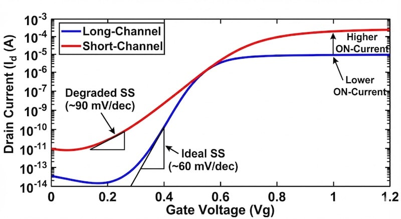
Figure 4. Conceptual comparison of SS degradation in short- and long-channel devices [3].
Velocity Saturation
Velocity saturation and quasi-ballistic transport effects change how short-channel devices behave when they are ON. The short-channel electric field becomes so strong that carriers reach a maximum velocity Vsat. The quadratic law, \(I_{ds} \propto (V_{gs} - V{th})^2\), is no longer valid for short-channel devices. Instead, carrier velocity saturation limits the drain current by transport velocity rather than mobility, as illustrated in Figure 5.
![Figure 5: Velocity saturation for holes and electrons [6].](https://www.allaboutcircuits.com/uploads/articles/Si-Vision_Nanoscale_Fig_5.jpg)
Figure 5. Velocity saturation for holes and electrons [6].
Short-channel devices have a broader taxonomy of challenges and can be presented in four categories:
- Electrostatic Control: Degraded by punch-through effects, reverse short-channel behavior, and narrow-width geometry effects.
- Carrier Transport: Limited by channel length modulation, surface roughness scattering, and impact ionization.
- Leakage Mechanisms: Increased by gate-induced drain leakage, gate oxide tunneling, and junction leakage currents.
- Reliability and Aging: Affected by hot carrier injection, bias temperature instability, and time-dependent dielectric breakdown.
Historical Evolution of Mitigation Strategies
The industry has countered SCEs through successive device and material shifts:
- 1990s — Channel Engineering: Halo/pocket implants suppress DIBL and punch-through by locally raising ; trade-offs include mobility loss and increased junction leakage.
- 2000s — Materials Innovation: HKMG at 45-nm node restores gate control by enabling low EOT with reduced tunneling leakage; strain engineering (e.g., SiGe S/D for PMOS) boosts mobility to offset short-channel transport degradation.
- 2010s — Architectural Shift (FinFET): FinFET/Tri-Gate at 22-nm node wraps the gate around multiple channel surfaces, strengthening electrostatics, reducing drain-field coupling, and extending scaling to 5 nm [7].
- 2020s and Beyond — Ultimate Enclosure (GAA): GAA nanosheets surround stacked channels on all sides, mitigating FinFET leakage paths (notably at the fin base) and providing maximal electrostatic control for 3-nm and 2-nm nodes [8].
Architectural Performance of FinFET and GAA Nanosheets
The mitigation of SCE towards 2 nm is no longer a one-size-fits-all approach. Modern foundries exploit their mastery of physical phenomena to offer distinct PPA (Power, Performance, Area) advantages. The following sections analyze how the leading players, Samsung, Intel, and TSMC, are architecting their devices to turn these physical constraints into competitive advantages.
FinFET vs. GAA
FinFETs at the 3 and 2 nm nodes have a degradation of electrostatic control, as the gate covers three sides of the channel, but the bottom of the fin is connected to the substrate leaving a potential leakage path. GAA devices completely surround the channel, maximizing the gate control. Table 1 compares FinFET and GAA metrics at the (3–5 nm) nodes.
Table 1. FinFET vs. GAA metrics at (3–5 nm) nodes [9, 10].
| Metric | FinFET | GAA Nanosheet | Improvement Factor | Physical Mechanism |
| DIBL | ~60–80 mV/V | ~30–45 mV/V | ~40–50% Reduction | Full channel shielding prevents drain field penetration. |
| Subthreshold Swing |
~75–85 mV/dec |
~65–70 mV/dec | ~15–20% Improvement |
Superior gate coupling factor and elimination of sub-fin leakage. |
| Leakage current |
1.0 (norm) | ~3.7x–4x Reduction |
Significant | Superior cutoff characteristics due to steeper SS. |
| Drive Current | 1.0 (norm) | ~1.3x Increase | 30% Increase | Larger effective width Weff per footprint due to vertical stacking. |
| Gate Controllability |
Moderate | High | Geometric Step | Due to the geometric factor N=4 vs N~=3 |
The 2 nm Landscape: Intel, TSMC, and Samsung
Samsung SF2: Multi-Bridge Channel FET (MBCFET)
Samsung led the industry implementation of GAA and introduced its MBCFET technology at the 3 nm node, with SF2 representing a second-generation refinement that enables fine-grained SCE optimization beyond FinFET capabilities [11]. The SF2 architecture emphasizes inner spacer engineering, a critical isolation layer between the source/drain extensions and gate stack, to improve electrostatic control. Optimized low-k inner spacers reduce parasitic overlap capacitances and suppress GIDL and punch-through paths [11, 13].
Additionally, MBCFET offers finer effective width granularity than fin-count–quantized FinFETs by allowing adjustable nanosheet geometries within process design-rule limits, enabling more targeted drive current sizing with reduced over-sizing penalties [12]. Figure 6 depicts the MBCFET structure.
![Figure 6. The MBCFET Structure [11].](https://www.allaboutcircuits.com/uploads/articles/Si-Vision_Nanoscale_Fig_6.jpg)
Figure 6. The MBCFET Structure [11].
Intel 18A: RibbonFET and PowerVia
Intel’s 18A node combines RibbonFET gate-all-around transistors with backside power delivery to address scaling limitations in electrostatic control and interconnect routing. As shown in Figure 7, RibbonFET employs vertically stacked nanosheet channels to increase effective channel width per footprint while enabling full gate enclosure, improving subthreshold swing to reported values on the order of ~65 mV/dec and reducing drain-induced barrier lowering through enhanced electrostatic shielding [14, 15].
In parallel, the PowerVia backside power delivery network relocates high-current power rails from front-side metal layers to the wafer backside, reducing routing congestion, improving signal integrity, and lowering resistive voltage drop. This vertical power delivery approach enables density scaling through reduced cell height rather than aggressive gate pitch shrinkage, preserving critical gate length and spacer dimensions required for short-channel effect suppression while meeting advanced-node area targets [16, 17].
![Figure 7. The RibbonFET transistor and the PowerVia backside
power-delivery [14].](https://www.allaboutcircuits.com/uploads/articles/Si-Vision_Nanoscale_Fig_7.jpg)
Figure 7. The RibbonFET transistor and the PowerVia backside power-delivery [14].
TSMC N2: Precision Geometry and Yield Focus
TSMC’s N2 node adopts a measured scaling strategy that prioritizes transistor yield stability and defect control by retaining front-side power delivery in its initial deployment. This approach decouples nanosheet device optimization from interconnect risk, allowing TSMC to focus on mastering GAA electrostatics without introducing the added process complexity of backside power rails [8, 18].
At the device level, N2 addresses SCEs through continuous effective width scaling enabled by variable nanosheet geometry. Unlike FinFETs, which rely on discrete fin counts and coarse width quantization, nanosheet width can be adjusted in fine increments, allowing precise drive current tuning while minimizing leakage and parasitic capacitance penalties associated with over-sizing.
However, at the layout level, the absence of backside power delivery preserves front-side routing congestion, creating scaling limitations in standard cell height due to competition between signal routing and power rails in the lower metal layers. As a result, while transistor electrostatics scale efficiently, overall cell footprint reduction remains constrained by interconnect density. Table 2 compares the leading 2-nm-class logic technologies.
Table 2. Comparison of Leading 2nm-Class Logic Technologies.
| Feature | TSMC N2 | INTEL 18A | Samsung SF2 |
| Architecture Name | NanoSheet | RibbonFET | MBCFET |
| Power Delivery | Frontside | Backside (PowerVia) | Frontside |
| Logic Density (Est.) [18] |
~313 MTr/mm2 | ~238 MTr/mm2 | ~231 MTr/mm2 |
| SCE Strategy | Continuous Weff (No Quantization) |
PowerVia (Vertical cell scaling) enables tighter pitch |
Inner Spacer Engineering (Low-k) |
Conclusion
The transition from planar transistors to GAA nanosheet architectures demonstrates the industry’s response to fundamental electrostatic scaling limits. While early SCEs were mitigated through process and doping optimization, continued dimensional scaling ultimately required architectural redesign. Experimental studies report reduced leakage and improved switching behavior in nanosheet devices relative to FinFETs under comparable operating conditions. This enhanced electrostatic control further enables system-level optimizations, such as backside power delivery, by relaxing layout-scaling constraints.
However, as device dimensions approach atomic limits, material properties increasingly dominate performance and variability. Sustained technology scaling will therefore depend not only on dimensional reduction, but on continued innovation in channel materials and three-dimensional device integration to preserve electrostatic integrity.
The featured image of the EXE5000 EUV scanner was used courtesy of ASML.
Acknowledgment
Sincere appreciation is extended to Fady Atef for performing a comprehensive review of the article and providing insightful comments.
References
[1] R. H. Dennard et al., "Design of ion-implanted MOSFET's with very small physical dimensions," IEEE Journal of Solid-State Circuits, vol. 9, no. 5, pp. 256–268, Oct. 1974.
[2] K. Rupp, “42 Years of Microprocessor Trend Data,” Karl Rupp’s Blog, 2018. [Online data is periodically updated]. Accessed: Nov. 20, 2025.
[3] C. Hu, "MOSFETs in ICs—Scaling, Leakage, and Other Topics," in Modern Semiconductor Devices for Integrated Circuits, Upper Saddle River, NJ: Prentice Hall, 2010, ch. 7.
[4] A. S. Roy, S. P. Mudanai and M. Stettler, "Mechanism of Long-Channel Drain-Induced Barrier Lowering in Halo MOSFETs," in IEEE Transactions on Electron Devices, vol. 58, no. 4, pp. 979-984, April 2011, doi: 10.1109/TED.2011.2109387
[5] B. G. Streetman and S. Banerjee, Solid State Electronic Devices, 7th ed. Upper Saddle River, NJ, USA: Pearson, 2014, ch. 6, p. 336.
[6] N. H. E. Weste and D. M. Harris, CMOS VLSI Design: A Circuits and Systems Perspective, 4th ed. Boston, MA, USA: Addison-Wesley, 2011, ch. 2, p. 76.
[7] Karimi, K.; Fardoost, A.; Javanmard, M., Comprehensive Review of FinFET Technology: History, Structure, Challenges, Innovations, and Emerging Sensing Applications. Micromachines 2024, 15, 1187.
[8] G. Yeap et al., "2nm Platform Technology Featuring Energy-Efficient Nanosheet Transistors and Interconnects Co-Optimized with 3DIC for AI, HPC and Mobile SoC Applications," 2024 IEEE International Electron Devices Meeting (IEDM), San Francisco, CA, USA, 2024, pp. 1-4, doi: 10.1109/IEDM50854.2024.10873475.
[9] G. Bae et al., "3nm GAA Technology featuring Multi-Bridge-Channel FET for Low Power and High-Performance Applications," 2018 IEEE International Electron Devices Meeting (IEDM), San Francisco, CA, USA, 2018, pp. 28.7.1-28.7.4, doi: 10.1109/IEDM.2018.8614629.
[10] Wang, D.; Sun, X.; Liu, T.; Chen, K.; Yang, J.; Wu, C.; Xu, M.; Zhang, W., "Investigation of Source/Drain Recess Engineering and Its Impacts on FinFET and GAA Nanosheet FET at 5 nm Node." Electronics 2023, 12, 770.
[11] Samsung Electronics, "Infographic: Reduced Size, Increased Performance: Samsung’s GAA Transistor, MBCFET™," Samsung Global Newsroom, Mar. 14, 2019.
[12] "3nm GAA MBCFET: Unrivaled SRAM Design Flexibility," Samsung Semiconductor Tech Blog, 2022.
[13] H. J. Lee et al., "Study of Silicon Nitride Inner Spacer Formation in Process of Gate-all-around Nano-Transistors," Nanomaterials, vol. 10, no. 5, p. 969, May 2020.
[14] Intel Foundry Services, “Intel 18A Process Node Platform Brief,” Intel Corporation, 2025.
[15] M. Radosavljević et al., "Demonstration of a Stacked CMOS Inverter at 60nm Gate Pitch with Power Via and Direct Backside Device Contacts," 2023 International Electron Devices Meeting (IEDM), San Francisco, CA, USA, 2023, pp. 1-4, doi: 10.1109/IEDM45741.2023.10413678.
[16] Wang, X., G. H. Baek, K. G. Bannore, et al., “A 0.021-μm² High-Density SRAM in Intel-18A RibbonFET Technology with PowerVia Backside Power Delivery,” presented in Session 29.2 (SRAM), IEEE International Solid-State Circuits Conference (ISSCC), San Francisco, CA, USA, Feb. 2025. (See ISSCC 2025 Session 29)
[17] W. Hafez et al., "Intel PowerVia Technology: Backside Power Delivery for High Density and High-Performance Computing," 2023 IEEE Symposium on VLSI Technology and Circuits (VLSI Technology and Circuits), Kyoto, Japan, 2023, pp. 1-2, doi: 10.23919/VLSITechnologyandCir57934.2023.10185208.
[18] D. Nenni, “IEDM 2025 – TSMC 2nm Process Disclosure – How Does it Measure Up?” SemiWiki/TechInsights, Feb. 2025.