Facebook
 Google
 GitHub
 Linkedin
Four Interesting AM Modulation Circuits You Should Know About
This article highlights a selection of circuits used for amplitude modulation, including a switching modulator built with just one diode and a circuit that incorporates a Class C power amplifier.
There are numerous ways to implement amplitude modulation (AM). So far, this article series has discussed four of them:
In this article, we’ll explore four more. We’ll start with a basic analog multiplier, then examine an alternative ring modulator configuration and a single-diode switching modulator. Finally, we’ll learn about the collector modulation circuit, which is sometimes classified as a switching modulator as well.
The Differential Pair Multiplier
Previous articles in this series introduced us to two types of AM signals. The first, known as double-sideband suppressed-carrier (DSB-SC) modulation, simply multiplies the message signal by a carrier wave. As the name ‘suppressed carrier’ suggests, the carrier wave does not appear in the transmitted spectrum. Equation 1 shows the modulated signal produced by this method.
$$s_{out}(t) ~=~ m(t)~\times~A_c \cos(\omega_c t)$$
Equation 1.
The second method, sometimes called conventional AM, retains the carrier wave in the transmitted spectrum. It does so by using the following equation to generate the modulated signal:
$$s_{out}(t) ~=~ A_c \Big ( 1~+~ \mu m(t) \Big ) \cos(\omega_c t)$$
Equation 2.
Analog multipliers can be used to directly compute output signals of either type. However, this article will mostly focus on generating AM signals with a transmitted carrier. Figure 1 illustrates two possible analog configurations for this purpose.
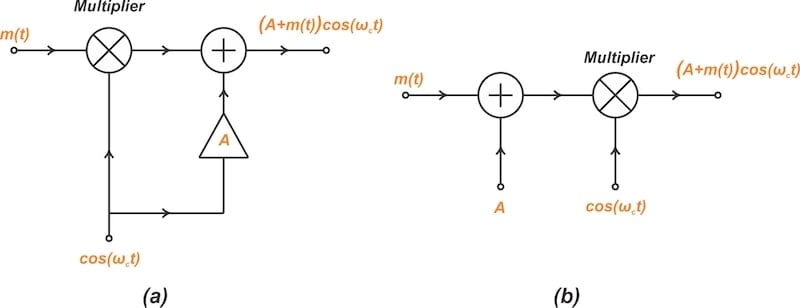
Figure 1. Two possible arrangements for generating conventional AM waves.
The addition operation in the figure above is implemented through an op amp summer (Figure 2).

Figure 2. The addition function can be achieved using an op amp summing circuit.
The analog multipliers are more difficult to implement. One method is to use a variable transconductance multiplier like the one in Figure 3.
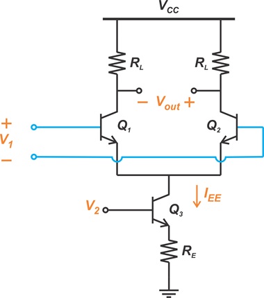
Figure 3. An emitter-coupled pair functions as a simple analog multiplier.
In the above circuit, one input (V1) is applied to the differential pair. The other input (V2) is used to control the current through the differential pair. Though a differential pair is a nonlinear circuit, for a small-signal V1 this circuit behaves as a constant-gain amplifier. If we assume that V1 is small and the bias current (IEE) is fixed, the output voltage can be expressed as:
$$V_{out} ~\approx~ g_m R_L V_1$$
Equation 3.
where gm, the transconductance, is given by:
$$g_m ~=~ \frac{I_c}{V_T} ~=~ \frac{I_{EE}}{2V_T} ~\approx~ \frac{V_2}{2R_E V_T}$$
Equation 4.
where VT is the thermal voltage.
By combining Equations 3 and 4, we obtain a new equation for the output voltage:
$$V_{out} ~\approx~ \frac{R_L}{2R_E V_T} ~\times~ V_1 V_2$$
Equation 5.
which shows that the output voltage is directly proportional to the product of the two input signals. Note, however, that this equation is valid only if V1 is small and V2 is much greater than the voltage drop across the base-emitter junction (about 0.7 V).
Due to these limitations, the emitter-coupled pair shown above isn’t employed in communication applications. However, it’s still an important circuit to know about. The Gilbert cell, which is the basis for most integrated circuit multipliers, is a modified version of the emitter-coupled pair. If you want to learn more about the Gilbert cell, I recommend the book Analysis and Design of Analog Integrated Circuits by Paul R. Gray.
While we can use analog multipliers to generate AM signals, they generally operate at low power levels and are limited to relatively low frequencies. Consequently, we typically use other techniques—switch-based circuitry, for example—to perform the necessary multiplication.
The Ring Modulator: An Alternative Implementation
A ring modulator is a form of switching modulator. During one half-cycle, it transmits the input signal to the output with its original polarity. During the alternate half-cycle, the signal is transmitted with inverted polarity. This results in amplitude-modulated signals at the carrier frequency (fc) and its harmonics. A bandpass filter tuned to the carrier frequency is incorporated at the output to extract the desired AM wave.
As the article introduction mentioned, we previously discussed ring modulators at length. However, Figure 4 shows a different configuration from the one we examined.
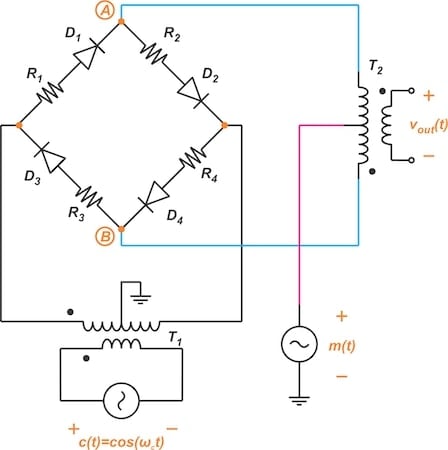
Figure 4. An alternative method of implementing a double-balanced ring modulator.
Both circuits implement the same basic concept: multiplying the message signal by a square wave that switches between ±1. As discussed in the previous article on ring modulators, this relaxes the bandpass filter’s transition band requirement and doubles the amplitude of the output signal when compared to a diode bridge modulator.
To better understand the operation of this circuit, let’s consider each half-cycle of the carrier wave (\(c(t)~=~ \cos(\omega_c t)\)) separately.
The Positive Half-Cycle
During the positive half-cycle of c(t), the diodes D1 and D2 are forward-biased and the diodes D3 and D4 are reverse-biased. Considering the symmetry of the circuit and noting that the center tap of T1 is grounded, this means that node A should also be at ground.
Clearly, this can be achieved only if both of the following are true:
- The diodes D1 and D2 and the resistors R1 and R2 are matched.
- The secondary of the transformer is accurately center-tapped.
During the positive half-cycle of c(t), the circuit schematic therefore simplifies to the one shown in Figure 5.

Figure 5. The simplified diagram of the ring modulator during the positive half-cycle of the carrier wave.
Applying the transformer dot convention to the figure above, we observe that the message signal appears at the output with its original polarity.
The Negative Half-Cycle
During the negative half-cycle of the carrier wave, diodes D3 and D4 are turned ON and diodes D1 and D2 are OFF. When that’s the case, the symmetry of the circuit forces node B to ground, leading to the simplified circuit in Figure 6.
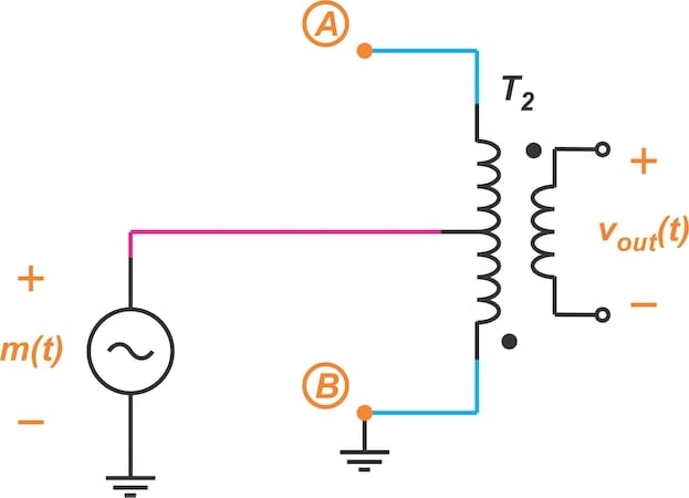
Figure 6. The simplified diagram of the ring modulator during the negative half-cycle of the carrier wave.
Here, m(t) is applied to the undotted end of the primary. The positive terminal of the output voltage is at the dotted end. As a result, the signal reaches the output with inverted polarity. Taken together with the positive half-cycle (Figure 5), we see that the configuration in Figure 4 multiplies the message signal by a square wave switching between ±1.
The Single-Diode Switching Modulator
Now that we understand the alternative ring modulator, let’s discuss how a single diode can be used to produce AM waves. Figure 7 shows the circuit diagram for this switching modulator.

Figure 7. The schematic of the single-diode switching modulator.
Here, the sum of m(t) and the carrier wave is applied to a diode in series with a resistor. We assume that the amplitude of the carrier wave (Ac) is much greater than the message signal (Ac ≫ m(t)). Under this condition, the diode acts as a switch that stays open during the negative half-cycle of c(t) and closes during its positive half-cycle. Neglecting the voltage drop across the diode, we can express the output voltage in terms of the voltage at node A (vA) as follows:
$$v_{out} ~=~\begin{cases} 0 & c(t) ~<~ 0 \\v_A & c(t) ~\geq~ 0 \end{cases}$$
Equation 6.
This is equivalent to multiplying vA by g(t), a square wave with a frequency of fc. Figure 8 shows g(t).
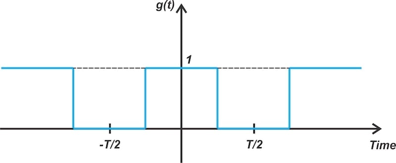
Figure 8. The square wave function g(t) that multiplies vA in the single-diode switching modulator.
The function g(t) can be expanded into a Fourier series consisting of cosine functions:
$$g(t) ~=~ \frac{1}{2}~+~ \frac{2}{\pi} \cos( \omega_c t) ~-~ \frac{2}{3 \pi} \cos( 3 \omega_c t) ~+~ \frac{2}{5 \pi} \cos(5 \omega_c t)~-~ \ldots$$
Equation 7.
The voltage at node A is given by:
$$v_A ~=~ m(t) ~+~ A_c \cos( \omega_c t)$$
Equation 8.
Multiplying vA by g(t) produces a vout with spectrum components centered at DC, the fundamental frequency (fc), and its harmonics. To separate the spectrum component centered at fc from the other ones, we express vout as:
$$v_{out} ~=~ \frac{1}{2} m(t) ~+~ \frac{1}{2}A_c \cos( \omega_c t) ~+~ \frac{2}{ \pi} m(t) \cos( \omega_c t) ~+~ \text{harmonic terms}$$
Equation 9.
A bandpass filter centered at fc then suppresses the DC and higher-frequency harmonic terms seen above. This provides the desired AM output signal:
$$s_{out} ~=~ \frac{1}{2}A_c \Big (1~+~ \frac{4}{ \pi} \frac{m(t)}{A_c} \Big ) \cos( \omega_c t)$$
Equation 10.
Single-Diode Modulator: Square-Law or Switching Modulator?
If you’ve been following this series, you may have noticed a resemblance between the switching modulator in Figure 7 and the square-law modulators we learned about in an earlier article. Before we move on to the next circuit, let’s take a moment to discuss this.
In a square-law modulator, the sum of the message and carrier waves are applied to a nonlinear device: a diode, a BJT, or a FET. The second-order nonlinearity of the nonlinear device generates a cross-product term, which is proportional to the product of the two functions. The nonlinear device is followed by a bandpass filter that separates the AM wave centered at the carrier frequency from the undesired components. This is illustrated in Figure 9.
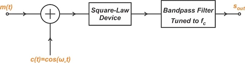
Figure 9. Block diagram of the square-law modulator.
Since the nonlinear characteristic can be achieved by incorporating a diode, what’s the difference between a square-law modulator built around a diode and the switching modulator shown in Figure 7? The answer lies in the modulators’ respective principles of operation.
A square-law modulator relies on the nonlinear characteristic of the device. If we represent the input-output characteristic of the nonlinear device by:
$$y(t) ~\approx~ \alpha_1 x(t) ~+~ \alpha_2 x^2(t)$$
Equation 11.
then the AM signal generated by the square-law modulator is:
$$s_{out} ~=~ \alpha_1 \Big ( 1 ~+~ 2 \frac{ \alpha_2}{\alpha_1} m(t) \Big ) \cos( \omega_c t); \quad \text{with} \quad \mu~=~2 \frac{ \alpha_2}{\alpha_1}$$
Equation 12.
In the above equation, the output signal depends on the linear and second-order coefficients (⍺1 and ⍺2) of the device’s input-output characteristic. The circuit in Figure 7, however, doesn’t rely on the nonlinearity of the diode. As Equation 6 shows, this circuit can generate AM waves even if the diode exhibits a perfectly linear characteristic during its ON-state.
The Collector Modulator
The last configuration we’ll discuss is the collector-modulated circuit in Figure 10. This AM modulator is commonly used in high-power transmitters for applications such as broadcasting.

Figure 10. The simplified schematic of a collector-modulated circuit.
In a collector modulator, the message signal is placed in series with the supply voltage of a Class C RF amplifier that’s driven into saturation. A positive message signal results in the amplifier receiving a higher collector voltage, which then produces a larger output signal. Conversely, a negative message signal leads to a lower collector voltage and a smaller amplifier output.
The output is bandpass-filtered to eliminate harmonics created by nonlinear operation of the transistor. The transistor acts as a switch driven at the carrier frequency.
Wrapping Up
We’ve now seen how amplitude modulation can be achieved using a variety of modulator circuits. Each of these has its own unique advantages and drawbacks. Analog multipliers, for example, have the benefit of simplicity. However, building an analog multiplier with a large dynamic range is much less simple, especially at high frequencies. Ring modulators are often associated with low-power modulation, whereas the collector-modulated circuit more readily lends itself to high-power transmitters.
This article is Part 8 of a series on amplitude modulation in RF systems. A complete list of articles in this series is provided below:
- Introduction to Modulation Techniques in RF Systems
- Understanding Double-Sideband Suppressed-Carrier Modulation
- Understanding Conventional Amplitude Modulation
- Understanding the Square-Law Modulator for Generating AM Signals
- Introduction to the Balanced Modulator for AM Signals
- How Do Switching Modulators Generate AM Signals?
- Understanding How Ring Modulators Produce AM Signals
- Four Interesting AM Modulation Circuits You Should Know About
- Demodulating Double-Sideband AM Signals
- Introduction to Single-Sideband Modulation: The Filter Method
- The Phasing Method and Hilbert Transforms for Single-Sideband Modulation
- A Visual Approach to Understanding the Phasing Method for SSB Modulation
- How Phasors Help Us Understand Bandpass Signals
- Introduction to Weaver’s Method for SSB Signal Generation
- Exploring the Operation of the Weaver Modulator for Single-Sideband Modulation
All images used courtesy of Steve Arar