Facebook
 Google
 GitHub
 Linkedin
Understanding How Ring Modulators Produce AM Signals
Among modulator circuits, the ring modulator stands out as one of the most effective for generating AM signals. Learn why in this article.
Amplitude-modulated (AM) signals can be generated using several types of modulator circuit. Switching modulators, for example, multiply the message signal by a periodic function with a fundamental frequency equal to the desired carrier wave frequency. This produces AM waves at the fundamental frequency and its harmonics. A bandpass filter then passes the desired spectrum component to the output.
We learned about one member of the switching modulator family, the diode bridge modulator, in the preceding article. In this article, we’ll delve into a different, higher-performing, switching modulator circuit: the ring modulator.
The Diode Bridge Modulator: A Review
Before proceeding, let's revisit the key aspects of the diode bridge modulator. This will help us to better understand the subtleties of the ring modulator and the performance improvement it offers over the diode bridge modulator.
With a diode bridge modulator, the message signal (m(t)) is multiplied by a square wave (g(t)) that switches between zero and one. This is shown in Figure 1.

Figure 1. The gating function used in a diode bridge modulator.
Assuming that the message signal is a single-tone sinusoidal wave, multiplication by the square wave produces the blue waveform in Figure 2.

Figure 2. The signal after applying the gating function (blue) and the resulting signal at the bandpass filter output (green).
To produce the final AM wave, we need to pass the blue waveform through a bandpass filter tuned to the carrier frequency (fc). This generates the green waveform in the above figure.
A mathematical analysis shows that the final signal at the filter output is given by:
$$s_{out}(t) ~=~ \frac{2}{\pi} m(t) \cos( \omega_c t)$$
Equation 1.
In the frequency domain, multiplication by the square wave shown in Figure 1 produces replicas of the message signal spectrum centered at 0, ±fc, ±3fc, ±5fc, etc, as illustrated in Figure 3.

Figure 3. The spectrum of the baseband message signal (a) and the signal produced by the modulator before applying the bandpass filter (b).
Now that we’ve reviewed the diode bridge modulator, let’s explore the ring modulator.
Operation of the Ring Modulator
Figure 4 shows the circuit schematic of a ring modulator. It uses four diodes arranged in such a way that they form a loop—the “ring” for which this configuration is named.
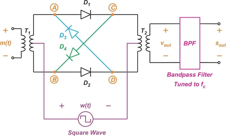
Figure 4. Schematic of a ring modulator.
At the bottom of Figure 4, we see a square wave (w(t)). This square wave, which has an amplitude of ±A1, is fed into the center taps of the transformers (T1 and T2) and switches at the fundamental frequency (fc).
When w(t) is a large positive value, the following is true:
- Diodes D1 and D2 are switched ON.
- The diodes in the cross-arm section (D3 and D4) are OFF.
- Node A is connected to node C.
- Node B is connected to node D.
In other words, during the positive half-cycle of w(t), the voltage across the secondary of T1 is transmitted to the primary of T2 with its original polarity.
When w(t) is a large negative value:
- Diodes D3 and D4 are switched ON.
- Diodes D1 and D2 are OFF.
- Node A is connected to node D.
- Node B is connected to node C.
The voltage across the secondary of T1 is therefore transmitted to the primary of T2 with inverted polarity during the negative half-cycle.
In effect, the ring modulator acts as a commutator, periodically reversing the voltage direction. Mathematically speaking, the message signal is multiplied by a square wave switching between ±1. This is illustrated in Figure 5.

Figure 5. The gating function used in the ring modulator.
Next, let’s consider the time-domain waveforms of this circuit.
Time-Domain Waveforms
As with the diode bridge modulator, we examine time-domain behavior by applying a single-tone sinusoidal message signal to the circuit. The top plot of Figure 6 shows the message signal; the bottom plot shows the waveform by which m(t) is multiplied due to the circuit operation.

Figure 6. The single-tone input applied to the ring modulator (top) and the waveform by which the message is effectively multiplied (bottom).
We’re assuming that both transformers have a turns ratio of unity and that all the diodes have a voltage drop of zero.
Figure 7 shows the output voltage (vout) we obtain by multiplying these waveforms together.

Figure 7. The output waveform (vout) generated by the ring modulator.
Like the diode bridge modulator, the ring modulator requires us to pass vout through a bandpass filter to generate the final AM wave. Applying an appropriate bandpass filter produces the green waveform in Figure 8.
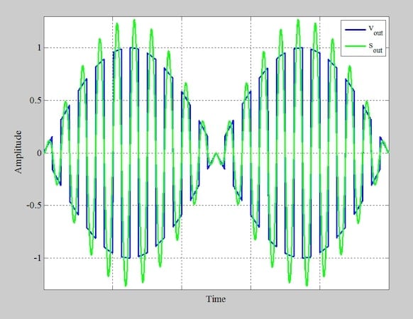
Figure 8. The signal after the gating function is applied (blue) and the final signal at the bandpass filter's output (green).
Deriving the Output Signal Equation
To derive an equation for the output signal, we note that the gating function depicted in Figure 5 (g(t)) can be expressed using the following Fourier series expansion:
$$g(t) ~=~ \frac{4}{\pi} \cos( \omega_c t) ~-~ \frac{4}{3 \pi} \cos( 3 \omega_c t) ~+~ \frac{4}{5 \pi} \cos(5 \omega_c t)~-~ \ldots$$
Equation 2.
Note that since g(t) is an even function, it can be expanded in terms of cosine functions only. The output voltage is:
$$v_{out} (t) ~=~ m(t) ~\times~ g(t)$$
Equation 3.
Combining the above equations yields:
$$v_{out}(t) ~=~ \frac{4}{\pi} m(t) \cos( \omega_c t) ~-~ \frac{4}{3 \pi} m(t) \cos( 3 \omega_c t) ~+~ \frac{4}{5 \pi} m(t) \cos(5 \omega_c t)~-~ \ldots$$
Equation 4.
Equation 4 shows that vout(t) is the superposition of AM waves centered at ⍵c, ±3⍵c, ±5⍵c, etc. This is illustrated below, in Figure 9.

Figure 9. The spectrum of the baseband message signal (a) and the signal produced by the ring modulator before applying the bandpass filter (b).
The circuit suppresses the carrier wave while retaining the sidebands that actually transmit the information. As we’ll touch on at the very end of the article, it’s also possible to retain the carrier wave when using a ring modulator. However, that’s largely beyond the scope of this discussion.
Returning to Figure 9, the desired spectrum is centered at fc. In order to separate it from the other spectrum components, we should have:
$$3f_c ~-~ B \geq f_c ~+~ B \quad \rightarrow \quad f_c ~\geq~ B$$
Equation 5.
This condition is readily achievable in practice, as the ratio of the carrier frequency to the baseband signal's bandwidth (fc/B) usually falls between 100 and 300.
To select the desired sidebands around ±fc, the ring modulator includes a bandpass filter. With an ideal bandpass filter, only the spectrum component centered at fc passes through to the output, leading to:
$$s_{out}(t) ~=~ \frac{4}{\pi} m(t) \cos( \omega_c t)$$
Equation 6.
Comparing the Diode Bridge and Ring Modulator
Now that we’ve examined the circuit, waveforms, and equations of the ring modulator, let’s discuss some important differences between it and the diode bridge modulator.
DC Component of the Gating Function
The diode bridge modulator’s gating function has a DC value of 0.5. As Figure 3 shows, multiplying the message signal by this gating function creates a replica of the spectrum of m(t) around zero frequency. To suppress this spectrum component, the diode bridge modulator’s filter should have a transition band of \((f_c ~–~ B) ~–~ B~\approx~f_c\).
The gating function of the ring modulator, on the other hand, doesn’t have a DC component. As a result, we see in Figure 9 that no spectrum component appears around zero frequency at the output. Instead, the closest spectrum component is centered at 3fc.
This affects the sharpness of the bandpass filter's transition band. To suppress the spectrum component centered at 3fc, the ring modulator requires a filter with a transition band of \(|(f_c~+~B)~-~(3f_c~-~B)|~\approx~2f_c\).
Symmetry of the Time-Domain Waveforms
To understand how the ring modulator eliminates the spectrum component centered at f = 0, consider its time domain waveforms. Examining these waveforms, we see that the signal produced by the ring modulator at the filter’s input is symmetrical about zero. This symmetry eliminates the message signal spectrum at zero frequency (DC).
This symmetry arises because the ring modulator outputs the message signal with either its original or inverted polarity during alternating half-cycles. By contrast, the signal produced by the diode bridge modulator is equal to the message signal during one half-cycle and drops to zero during the other.
Double-Balanced vs. Single-Balanced
At the input of the bandpass filter, the ring modulator generates only the product term. It suppresses both the message and carrier signals. Because it cancels out both the baseband signal and the carrier wave, we refer to the ring modulator as double-balanced.
The diode bridge modulator, on the other hand, is only balanced with respect to the carrier wave input. The message signal appears at the input of the bandpass filter, making it a single-balanced modulator.
Output Voltage Level
Comparing Equations 1 and 6, we observe that the output voltage produced by the ring modulator is double that of the diode bridge modulator. This is consistent with the green waveforms shown in Figures 2 and 8. These figures show AM waves with maximum amplitudes of 0.63 and 1.26, respectively.
Wrapping Up
The ring modulator transmits the input signal to the output with its original polarity during one half-cycle, and with inverted polarity during the alternate half-cycle. This relaxes the bandpass filter’s transition band requirement and doubles the amplitude of the output signal. It should be noted that preventing the carrier power from leaking into the ring modulator’s output requires perfectly balanced transformers and matched diodes.
As an aside, the ring modulator can also be used to generate AM signals that don’t suppress the carrier wave. To understand how, we note that the ring modulator effectively acts as a multiplier. Since no restriction has been placed on the input message signal, we can produce conventional AM signals by applying 1 + μm(t) with an arbitrary modulation index to the ring modulator.
This article is Part 7 of a series on amplitude modulation in RF systems. A complete list of articles in this series is provided below:
- Introduction to Modulation Techniques in RF Systems
- Understanding Double-Sideband Suppressed-Carrier Modulation
- Understanding Conventional Amplitude Modulation
- Understanding the Square-Law Modulator for Generating AM Signals
- Introduction to the Balanced Modulator for AM Signals
- How Do Switching Modulators Generate AM Signals?
- Understanding How Ring Modulators Produce AM Signals
- Four Interesting AM Modulation Circuits You Should Know About
- Demodulating Double-Sideband AM Signals
- Introduction to Single-Sideband Modulation: The Filter Method
- The Phasing Method and Hilbert Transforms for Single-Sideband Modulation
- A Visual Approach to Understanding the Phasing Method for SSB Modulation
- How Phasors Help Us Understand Bandpass Signals
- Introduction to Weaver’s Method for SSB Signal Generation
- Exploring the Operation of the Weaver Modulator for Single-Sideband Modulation
All images used courtesy of Steve Arar