Facebook
 Google
 GitHub
 Linkedin
Introduction to the Balanced Modulator for AM Signals
Learn how the balanced modulator addresses shortcomings of the square-law modulator when generating DSB-SC and conventional AM signals.
In the previous article of this series, we learned how square-law modulators utilize the second-order nonlinearity of electronic components to generate AM waves. In theory, this type of modulator circuit can produce both conventional AM and double-sideband suppressed-carrier (DSB-SC) signals. However, it can only produce DSB-SC signals if the linear term in the nonlinear element’s input-output characteristic is zero.
In practice, the linear term is typically non-zero. Furthermore, the cubic nonlinearity of practical nonlinear elements can generate undesired signal components at the output of the square-law modulator. This is true even when generating conventional AM signals.
In this article, we’ll discuss how to get around these issues by using two square-law devices in a balanced configuration. This arrangement, known as the balanced modulator, can generate both DSB-SC and conventional AM signals. Before we dive in, however, let’s review the square-law modulator and its limitations in a bit more detail.
Limitations of the The Square-Law Modulator
The square-law modulator in Figure 1 produces AM waves by sending the sum of m(t), the message signal, and c(t), the carrier wave, through a nonlinear device followed by a properly tuned bandpass filter.
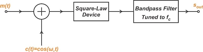
Figure 1. Block diagram of the square-law modulator.
In the preceding article, we assumed that the input-output characteristic of the square-law device in Figure 1 was represented by:
$$y(t) ~\approx~ \alpha_1 x(t) ~+~ \alpha_2 x^2(t)$$
Equation 1.
In which case the conventional AM signal at the output is given by:
$$s_{out} ~=~ \alpha_1 \Big ( 1 + 2 \frac{ \alpha_2}{\alpha_1} m(t) \Big ) \cos( \omega_c t)$$
Equation 2.
where the modulation index is:
$$\mu~=~2 \frac{ \alpha_2}{\alpha_1}$$
Equation 3.
Unless α1 = 0 in Equation 1, the square-law modulator can’t generate a DSB-SC signal. As mentioned previously, this won’t happen in practice.
The other limitation of Equation 1 is that it includes only α1 and α2. Meanwhile, practical nonlinear devices often contain nonlinearity terms beyond the second order in their power series expansions. These higher-order terms can generate undesired components at the output of the modulator.
To understand this, assume that the input-output characteristic of the nonlinear device can be represented by:
$$y(t) ~\approx~ \alpha_1 x(t) ~+~ \alpha_2 x^2(t) ~+~ \alpha_3 x^3(t)$$
Equation 4.
Equation 5 shows the components that appear at the output if we pass (m(t) + cos(⍵ct)) through the cubic term in Equation 4:
$$\begin{gather*}\alpha_3 \big ( m(t) ~+~ \cos(\omega_c t) \big ) ^3 ~=~ \\\alpha_3 m^3(t) ~+~ 3 \alpha_3 m^2(t) \cos (\omega_c t)~+~3 \alpha_3 m(t) \cos^2(\omega_c t)~+~\alpha_3 \cos^3( \omega_c t)\end{gather*}$$
Equation 5.
We can break down the results of this equation as follows:
- The first term, \(\alpha_3m^3(t)\), generates a spectrum component centered at f = 0.
- The second term, \(3 \alpha_3m^3(t) \cos(\omega_ct)\), is centered at f = fc.
- The third term, \(3 \alpha_3m^3(t) \cos^2 (\omega_ct)\), produces a DC component along with a component around the second harmonic (2fc).
- The fourth term, \(\alpha_3 \cos^3 (\omega_ct)\), produces components at the fundamental (fc) and third (3fc) harmonics.
Let’s use the trigonometric identity in Equation 6 to take a closer look at the fourth term.
$$\cos^3 (x) ~=~ \frac{1}{4} \cos(3x) ~+~ \frac{3}{4} \cos(x)$$
Equation 6.
Since the nonlinear device is followed by a bandpass filter tuned to fc, this cubic term produces the following additional components around the carrier frequency:
$$3 \alpha_3 m^2(t) \cos( \omega_c t) ~+~ \frac{3}{4} \alpha_3 \cos( \omega_c t)$$
Equation 7.
The first term of Equation 7 adds the square of the message signal translated in frequency by fc to the desired AM wave. Since this component interferes with the AM wave, it’s desirable to have a nonlinear device whose higher-order coefficients (⍺n for n ≥ 3) are negligible compared to ⍺2. Otherwise, we need to limit the input signal’s amplitude to keep the higher-order nonlinearity terms relatively small.
Using a balanced modulator is another option. In the next section, we’ll introduce the basic principles of the balanced modulator and explain how it generates DSB-SC signals. We’ll circle back to discuss how it deals with the abovementioned unwanted signal components later on in the article.
Using the Balanced Modulator to Produce DSB-SC Signals
Figure 2 shows the block diagram of a balanced modulator.
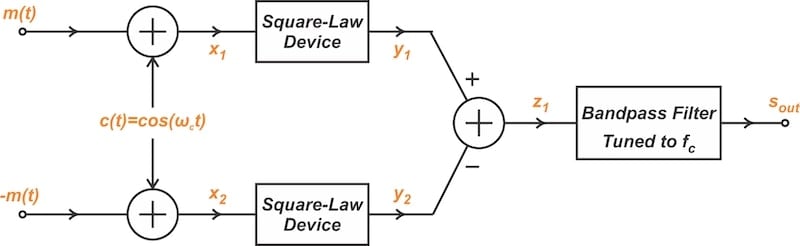
Figure 2. Block diagram of a balanced modulator.
As you can see, the balanced modulator incorporates two identical square-law modulators—one for each of the balanced modulator’s two signal paths. One path receives m(t), the message signal; the other path is fed the message signal’s inverted form, –m(t). The output signals from the nonlinear devices are subtracted from each other, and the resulting signal is then passed through a bandpass filter.
To see how the balanced configuration can produce DSB-SC signals even with ⍺1 ≠ 0, let’s set aside the cubic nonlinearity of the devices for now. The input-output characteristics of the nonlinear elements can therefore be described by:
$$y(t) ~\approx~ \alpha_1 x(t) ~+~ \alpha_2 x^2(t)$$
Equation 8.
The signals at the outputs of the two adders at the left side of Figure 2 are:
$$x_1 ~=~ m(t) ~+~ \cos( \omega_c t) \quad \text{and} \quad x_2 ~=~ -m(t)~+~\cos( \omega_c t)$$
Equation 9.
Combining Equations 8 and 9, the signal at the output of the upper nonlinear device is:
$$y_1(t) ~\approx~ \alpha_1 m(t) ~+~ \alpha_2 m^2(t) ~+~ \alpha_2 \cos^2( \omega_c t) ~+~ \Big ( \alpha_1 ~+~ 2 \alpha_2 m(t) \Big ) \cos( \omega_c t)$$
Equation 10.
Replacing m(t) with –m(t) in the above equation yields the signal at the output of the lower nonlinear device:
$$y_2(t) ~\approx~ -\alpha_1 m(t) ~+~ \alpha_2 m^2(t) ~+~ \alpha_2 \cos^2( \omega_c t) ~+~ \Big ( \alpha_1 ~-~ 2 \alpha_2 m(t) \Big ) \cos( \omega_c t)$$
Equation 11.
Subtracting y2(t) from y1(t), we obtain the signal z1(t):
$$z_1(t) ~=~ y_1(t) ~-~ y_2(t)~=~ 2\alpha_1 m(t) ~+~ 4 \alpha_2 m(t) \cos( \omega_c t)$$
Equation 12.
In the above equation, the first term is a baseband signal. The second term is the desired DSB-SC signal, which is centered around fc. The bandpass filter is tuned to fc and allows only the AM signal to pass through to the output, producing the following equation:
$$s_{out}(t) ~=~ 4 \alpha_2 m(t) \cos( \omega_c t)$$
Equation 13.
This is a DSB-SC signal, so the carrier that was applied to the input doesn’t appear at the output of the last adder. Instead, the circuit acts like a balanced bridge with respect to the input c(t) = cos(⍵ct)). The other input of the circuit, m(t), appears at node z1 (Equation 12).
Because it’s balanced with respect to only one of its inputs, we refer to the circuit as a single-balanced modulator. In a double-balanced modulator, both inputs are canceled out. Only the product of the message signal and carrier wave is available at the output.
Effect of Higher Order Nonlinearity Terms on the Balanced Modulator
Next, let’s see what happens when the nonlinear devices include cubic terms in their power series expansion. The cubic term generates the following undesired signal components at node y1:
$$3 \alpha_3 m^2(t) \cos( \omega_c t) ~+~ \frac{3}{4} \alpha_3 \cos( \omega_c t)$$
Equation 14.
To find the undesired signal components produced by the lower path, we should replace m(t) with –m(t) in the above equation. However, it’s clear that inverting the message signal doesn’t affect the undesired terms. Instead, because the undesired terms are present at both nodes y1 and y2, they cancel out at the output upon subtraction.
Note that the two nonlinear devices in a balanced modulator should exhibit approximately identical characteristics. Otherwise they won’t be able to eliminate the undesired signal components.
Generating Conventional AM Signals With a Balanced Modulator
So far, we’ve only discussed the balanced modulator in terms of DSB-SC signals. But what about conventional AM?
Equation 15 reproduces the basic equation for generating a conventional AM signal:
$$s_{out}(t) ~=~ A_c \Big ( 1~+~ \mu m(t) \Big ) \cos(\omega_c t)$$
Equation 15.
To adapt this equation for the balanced modulator, we note the following:
- The balanced modulator effectively acts as a multiplier.
- Our analysis of the balanced modulator places no restriction on the input message signal.
Given the above, we can ideally apply 1 + μm(t) with an arbitrary modulation index to the balanced modulator to produce conventional AM signals. This is shown in Figure 3.
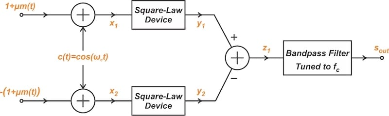
Figure 3. Using a balanced modulator to generate conventional AM signals.
Substituting 1 + μm(t) for m(t) in Equation 13, the output of the above circuit is:
$$s_{out}(t) ~=~ 4 \alpha_2 \big ( 1~+~ \mu m(t) \big ) \cos( \omega_c t)$$
Equation 16.
which is a conventional AM wave.
When using the balanced modulator to create conventional AM signals, it’s important to keep in mind that practical nonlinear elements may exhibit a square-law characteristic for a specific range of input values. For instance, the output of a nonlinear component might be proportional to the square of the input only when the input is positive.
If that’s the case, we need to restrict the nonlinear element’s input to the range where the device exhibits the expected square-law response. This limits the modulation index we can achieve when using the technique in Figure 3. However, we can increase the modulation index as needed by limiting the input signal to the permissible range and then subtracting an appropriately scaled version of the carrier wave from sout(t) at the output of the modulator.
A Practical Balanced Modulator Circuit
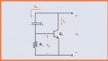
Let’s wrap up our discussion by briefly examining an example circuit implementation (Figure 4).

Figure 4. Example circuit implementation of the balanced modulator.
This circuit uses transformers to combine the carrier wave with the message signal. The required bandpass filter takes the form of an LC tank tuned to the carrier frequency at the modulator’s output. To introduce the required nonlinearity, diodes are used.
The currents through the diodes in Figure 4 exhibit a nonlinear relationship with the voltages across them. To understand this, let’s assume that the voltage at node C is much smaller than the voltage at node A. If that’s the case, we can approximate the voltage across the diode by the voltage at node A (vA). The current through the diode (I1) can then be described using a power series:
$$I_1 ~=~ \alpha_1 v_A ~+~ \alpha_2 (v_A)^2 ~+~ \alpha_3 (v_A)^3$$
Equation 17.
which is identical to the third-degree expression we used in our analysis of the generic balanced modulator earlier on.
Key Takeaways
We can use two square-law devices in a balanced configuration to generate either DSB-SC or conventional AM signals. In the latter case, however, the input range limitations of the nonlinear element can restrict the achievable modulation index. Still, the balanced modulator retains an important advantage over the square-law modulator—it eliminates the (potentially significant) undesired signal components produced by practical nonlinear elements.
This article is Part 5 of a series on amplitude modulation in RF systems. A complete list of articles in this series is provided below:
- Introduction to Modulation Techniques in RF Systems
- Understanding Double-Sideband Suppressed-Carrier Modulation
- Understanding Conventional Amplitude Modulation
- Understanding the Square-Law Modulator for Generating AM Signals
- Introduction to the Balanced Modulator for AM Signals
- How Do Switching Modulators Generate AM Signals?
- Understanding How Ring Modulators Produce AM Signals
- Four Interesting AM Modulation Circuits You Should Know About
- Demodulating Double-Sideband AM Signals
- Introduction to Single-Sideband Modulation: The Filter Method
- The Phasing Method and Hilbert Transforms for Single-Sideband Modulation
- A Visual Approach to Understanding the Phasing Method for SSB Modulation
- How Phasors Help Us Understand Bandpass Signals
- Introduction to Weaver’s Method for SSB Signal Generation
- Exploring the Operation of the Weaver Modulator for Single-Sideband Modulation
All images used courtesy of Steve Arar
Related Content