Facebook
 Google
 GitHub
 Linkedin
How Do Switching Modulators Generate AM Signals?
Using the example of a diode-bridge modulator, we examine the basic principles of switching modulators for AM signal generation.
Linear time-invariant (LTI) systems can’t generate frequencies other than those present in the input signal. Since modulation shifts input frequencies to a different range at the output, it requires circuits that are nonlinear, time-varying, or both. As a result, modulator circuits may be less familiar to many electrical engineers who are primarily engaged in the analysis and design of LTI systems.
To help correct this knowledge gap, previous articles in this series introduced the basics of square-law modulators and balanced modulators. Both of these are multiplier-based circuits. In this article, we’ll briefly review the multiplier-based modulators and then turn our attention to switching modulators. We’ll wrap up our discussion with some guidance on simulating a bandpass filter in MATLAB.
Modulation Methods and Multipliers: A Review
So far in this series, we’ve discussed two types of amplitude modulation (AM):
With DSB-SC modulation, the modulated signal, s(t), is produced by multiplying the message signal, m(t), by the sinusoidal carrier wave, c(t) = Accos(ωct):
$$s(t) ~=~ m(t) ~\times~ A_c \cos(\omega_c t)$$
Equation 1.
Conventional AM, which retains the carrier wave in the transmitted spectrum, uses the following equation:
$$s(t) ~=~ A_c \Big ( 1~+~ \mu m(t) \Big ) \cos(\omega_c t)$$
Equation 2.
We can use an analog multiplier to directly compute the output signals described by Equations 1 and 2. For example, Figure 1 illustrates two possible configurations for generating conventional AM signals.

Figure 1. Two possible arrangements for generating conventional AM waves.
We can implement analog multiplication using Gilbert cells, Hall effect devices, or log/anti-log amplifiers. However, most analog multipliers operate at low power levels and are limited to relatively low frequencies. At high frequencies, building an analog multiplier with a sufficiently large dynamic range is far from straightforward.
The Key Idea Behind Switching Modulators
Alternatively, we can use switch-based circuitry to perform the necessary multiplication. The key idea behind this type of modulator is that multiplication of the message signal m(t) by any periodic function g(t) with fundamental frequency fc produces AM waves at fc and its harmonics. If we assume that g(t) is an even periodic function with fundamental frequency fc, we can expand it into a Fourier series of the form:
$$g(t) ~=~ \sum_{n=0}^{n= \infty} a_n \cos(n \omega_c t ~+~ \theta_n)$$
Equation 3.
Multiplying the message signal by g(t), we have:
$$m(t) ~\times~ g(t) ~=~ \sum_{n=0}^{n= \infty} a_n m(t) \cos(n \omega_c t ~+~ \theta_n)$$
Equation 4.
The signal in Equation 4 is a superposition of AM waves centered at ⍵c, 2⍵c, 3⍵c, etc. This equation shows that we can generate AM waves by multiplying the message signal by any periodic function g(t) with fundamental frequency fc. It's therefore not essential to multiply m(t) by a pure sinusoidal wave to generate AM waves. Instead, we can opt for a more suitable function g(t) that makes the circuit implementation easier.
Interestingly, if g(t) is a square wave alternating between zero and one, it acts as a gating function that periodically turns the input ON and OFF. In this case, we can simplify multiplication to a switching operation. Figure 2 shows how this gating function can be implemented by means of a single switch.

Figure 2. A single switch can be used to multiply the input by a square wave.
In the above circuit, Rs models the source resistance. When the switch is open, the input is delivered to the output. When the switch is closed, the output drops to zero. The message signal is therefore multiplied by a square wave switching between zero and one (Figure 3).
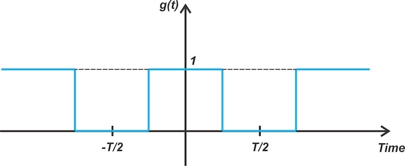
Figure 3. The gating function used in the switching modulator above.
We’ll discuss the implementation of this idea in more depth later on in the article. Before that, however, let’s examine the typical time-domain waveforms of the circuit.
The Switching Modulator’s Time-Domain Waveforms
To examine the time-domain behavior, we apply a single-tone sinusoidal message to the circuit. Figure 4 shows the message signal (top) as well as the waveform by which m(t) is multiplied (bottom).

Figure 4. The single-tone input applied to the modulator (top) and the waveform by which the message is effectively multiplied (bottom).
By multiplying these waveforms together, we obtain the output voltage in Figure 5.

Figure 5. The output waveform (vout) generated by the modulator.
As anticipated, the output voltage matches the message signal during one half of each cycle and drops to zero during the other half.
Although the amplitude of this waveform resembles the message signal, it isn't a typical amplitude-modulated signal. To produce the desired AM signal, we pass vout through a bandpass filter tuned to the carrier frequency. This is illustrated in Figure 6.

Figure 6. The signal after applying the gating function (blue) and the resulting signal at the bandpass filter output (green).
I'll provide a code excerpt at the end of the article to help you carry out the necessary filtering in MATLAB.
Circuit Implementation: the Diode Bridge Modulator
Figure 7 shows how we can implement the modulator’s switching function using a diode bridge.

Figure 7. A diode bridge can be used to build a switching modulator.
When c(t) is a large positive value, all four diodes conduct. With diodes D1 and D2 being matched, and diodes D3 and D4 likewise being matched, nodes A and B are at the same potential. As a result, nodes A and B are effectively shorted together when c(t) is a positive value. When c(t) is negative, all four diodes are open-circuited, emulating an open switch between nodes A and B.
The maximum switching frequency is dictated by how quickly the diodes can be turned ON and OFF.
Deriving the Diode Bridge Modulator’s Output Signal Equation
By assuming that g(t) is a square wave switching between zero and one, we can use the Fourier series representation to expand it in terms of cosine functions:
$$g(t) ~=~ \frac{1}{2}~+~ \frac{2}{\pi} \cos( \omega_c t) ~-~ \frac{2}{3 \pi} \cos( 3 \omega_c t) ~+~ \frac{2}{5 \pi} \cos(5 \omega_c t)~-~ \ldots$$
Equation 5.
Hence, the output voltage is:
$$v_{out}~=~ \frac{1}{2} m(t)~+~ \frac{2}{\pi} m(t) \cos( \omega_c t) ~-~ \frac{2}{3 \pi} m(t) \cos( 3 \omega_c t) ~+~ \frac{2}{5 \pi} m(t) \cos(5 \omega_c t)~-~ \ldots$$
Equation 6.
The output spectrum comprises replicas of the message spectrum centered at 0, ±fc, ±3fc, ±5fc, etc. This is illustrated in Figure 8(b) The spectrum of the baseband spectrum is shown in Figure 8(a).

Figure 8. The spectrum of the baseband message signal (a) and the signal produced by the modulator (b).
The output spectrum in Figure 8(b) includes several signals that we don’t want along with the one we do. Before we reach the final output equation, we need to filter out the undesired signal components.
Filtering to Isolate the AM Signal
In order to separate the desired spectrum centered at fc from the other spectrum components, we should have:
$$f_c ~-~ B \geq B \quad \rightarrow \quad f_c ~\geq~ 2B$$
Equation 7.
where B is the baseband signal’s bandwidth. Thus, we need to pass the output signal through a bandpass filter of bandwidth 2B, centered at fc to separate out the desired component (Figure 9).
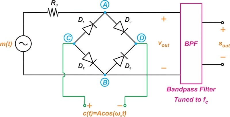
Figure 9. Schematic of a diode bridge modulator with bandpass filter.
With an ideal bandpass filter, only the spectrum component centered at fc passes through to the output, leading to:
$$s(t) ~=~ \frac{2}{\pi} m(t) \cos( \omega_c t)$$
Equation 8.
Let’s use the waveforms shown in Figure 6 to verify this equation. The modulated signal shown in the figure is obtained for a single-tone sinusoidal message with an amplitude of one. For |m(t)| ≤ 1, Equation 8 predicts the maximum value of the modulated signal to be about 2/π ≈ 0.64. This agrees well with the green waveform in Figure 6, which has a maximum value of about 0.63.
In the above discussion, we used a filter tuned to the carrier frequency to separate the spectrum component at fc. While we can tune the bandpass filter to a harmonic frequency to produce AM waves at that higher frequency, we typically prefer to use the component at the fundamental frequency because the Fourier coefficients decrease as we move to higher harmonics (see Equation 5).
MATLAB Simulation of a Bandpass Filter
I generated the time-domain waveforms in Figures 4 through 6 using MATLAB. If you’d like to recreate these waveforms and experiment on your own, I’ve included the code I used for the filtering process here. Otherwise, creating a bandpass filter can be a bit tricky for beginners.
The following code creates an ideal bandpass filter with sharp edges and unity gain by defining the frequency response (H) and applying it to your AM signal in the frequency domain. You’ll need to adjust the cutoff frequencies (fc1, fc2) and the sampling frequency (fs) based on the parameters of your specific example.
% Define parameters
fs = 10000; % Sampling frequency in Hz
fc1 = 900; % Lower cutoff frequency in Hz
fc2 = 1100; % Upper cutoff frequency in Hz
N = length(yourAMSignal); % Length of the signal

% Create the frequency axis
f = linspace(-fs/2, fs/2, N);

% Create the ideal bandpass filter frequency response
H = zeros(1, N);
H(abs(f) >= fc1 & abs(f) <= fc2) = 1;

% Apply the filter in the frequency domain
Y = fftshift(fft(yourAMSignal));
Y_filtered = Y .* H;
filteredSignal = ifft(ifftshift(Y_filtered));

% Plot the original and filtered signals
figure;
subplot(2,1,1);
plot(yourAMSignal); title('Original AM Signal'); subplot(2,1,2);
plot(real(filteredSignal)); title('Filtered Signal');
Wrapping Up
While we can use analog multipliers to generate AM signals, building an analog multiplier with a large dynamic range is tricky. This is especially true at high frequencies. The switching modulator is based on the idea that multiplying the input by any periodic function can generate AM waves at the fundamental and harmonic frequencies of the periodic function.
To help us understand how a switching modulator can operate in practice, this article introduced the diode bridge modulator. In the next article, we’ll discuss another switching modulator circuit: the ring modulator.
This article is Part 6 of a series on amplitude modulation in RF systems. A complete list of articles in this series is provided below:
- Introduction to Modulation Techniques in RF Systems
- Understanding Double-Sideband Suppressed-Carrier Modulation
- Understanding Conventional Amplitude Modulation
- Understanding the Square-Law Modulator for Generating AM Signals
- Introduction to the Balanced Modulator for AM Signals
- How Do Switching Modulators Generate AM Signals?
- Understanding How Ring Modulators Produce AM Signals
- Four Interesting AM Modulation Circuits You Should Know About
- Demodulating Double-Sideband AM Signals
- Introduction to Single-Sideband Modulation: The Filter Method
- The Phasing Method and Hilbert Transforms for Single-Sideband Modulation
- A Visual Approach to Understanding the Phasing Method for SSB Modulation
- How Phasors Help Us Understand Bandpass Signals
- Introduction to Weaver’s Method for SSB Signal Generation
- Exploring the Operation of the Weaver Modulator for Single-Sideband Modulation
All images used courtesy of Steve Arar