 Facebook
 Google
 GitHub
 Linkedin
Error Checking Schematics
This article presents tools and practices in reducing errors in your schematics.
This article presents tools and practices in reducing errors in your schematics.
Whether a schematic is used to assemble a circuit by hand, such as on a breadboard, or used to produce a printed circuit board, it is a vital step in the physical production of a circuit. To prevent expensive and time-consuming debugging, rework or revision of PCBs, a schematic should be as accurate and complete as possible before building the circuit or starting PCB layout.
This article presents tools and practices I have used over the years to reduce errors and produce a schematic which is accurate and complete. My experience is with less expensive or free schematic capture programs. My world is populated with OrCADs, KiCADs, Eagles, and similar creatures.
I do not discuss capabilities found in high-end EDA suites which have not migrated to lower-end tools.
Accurate Schematics Start with Accurate and Complete Symbols
The foundation of an error-free schematic is accurate symbols. It is important to be proficient with the symbol editor in your schematic capture software. Even if you do not have to personally create symbols, you will need to view and check the properties of symbols. Let’s explore what I mean by an accurate and complete symbol.
All pins of the part need to be visible in the symbol. If there are 44 pins on the part, there should be 44 pins visible on the symbol. I never use “invisible” pins such as power and ground pins. Also, “No Connect” pins are always shown. I will discuss two types of “No Connects”. The first type of “No Connect” are pins which should never be connected. They may not be connected within the part or they may be used for testing by the manufacturer.
U3 in this schematic has three pins (9, 10, 15) which are never to be connected and always left “open”. This particular schematic program allows a “Not Connected” type to be assigned to a pin as part of the symbol. So, these pins are permanently marked with a little “x”. I give them unique names, NC1, NC2, etc., as shown in the schematic. Schematic programs generally allow duplicate names, for example “VCC”. However, I always give “No Connects” unique names by adding a number to a base name of “NC”.
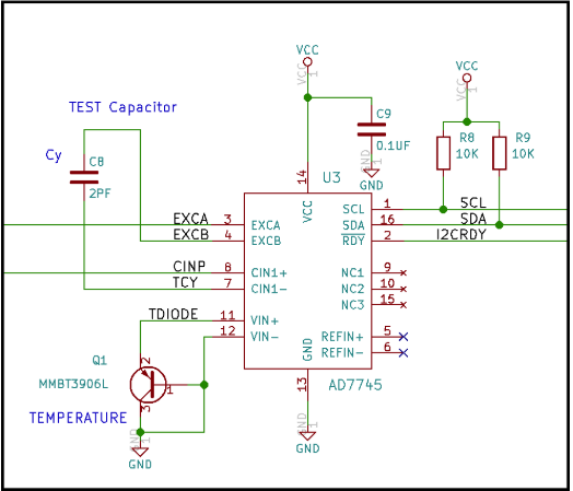
The second type of “No Connects” are pins which may be connected but are not connected in a particular design. For example, pins 5 and 6 may be connected to something but, in this design, are not connected. Many schematic programs allow an unconnected pin to be marked by placing a “Not Connected” schematic symbol, usually an “X”, as part of the schematic. If the program does not have the “Not Connected” symbol, any warnings or errors produced by an open pin can be ignored.
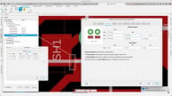
An important part of building an accurate symbol is assigning correct “electrical types” to every pin. These pin types are used by ERC or Electrical Rules Checking which is covered later. Adding a “type” to the pin is done with a menu such as the one shown below. The Electrical Type selection shows a list of typical electrical characteristics for a pin.

Sometimes, it takes a little creativity to select the correct type. Pick the one which is closest. If no choice makes sense, I often select “Passive” which effectively bypasses the ERC process. Not all programs will have the “Not Connected” type. If not available, I select a type which is likely to cause an ERC error if it is connected to something. This depends on how you set up the ERC rules.
Connectors, FPGAs and microcontrollers are parts where the symbol will need to be modified to assign a proper electrical type to many pins because the type is design dependent. Modify the pin types as signals are assigned to pins.
My final step in creating a symbol is finding a quiet place with no distractions and sitting down with the symbol editor and datasheets. I go around each part and carefully check each pin for a correct number, name and electrical type. Make sure all pins are there. It is a good idea to check the symbols as part of final checks when the schematic is done.
Putting some time between the creation of the symbol and the final check may keep you from repeating an error.
Electrical Rules Checking
ERC or Electrical Rules Checking is a utility which looks for incorrect connections based on a set of rules. Generally, the rules look for open pins or connections between incompatible types of pins. Generally, the rules are specified with a “Connection Matrix”.
Here is an example:

There is a row and a column in the matrix for each type which can be assigned to a pin. Every combination of pins defined by the intersection of a row and column is assigned a rule. In this case, a green element in the matrix means a connection between the two types of pins is allowed. A “W” produces a warning in the report. An “E” produces an error in the report. There is always a default matrix with a common set of rules. However, the matrix may have to be changed for your circuit.
ERC has limitations. The pin type for every pin on all parts must be accurate and meaningful. Then, the rules matrix must be meaningful for a particular circuit. Even with limitations, run ERC on the schematic! Modify the rules matrix for your circuit and modify the schematic until all the warnings and errors are gone.
How to Check a Net List
I always perform a manual scan of the netlist. There may be some disagreement regarding the necessity of this check but I have found errors which passed other checks. To me, finding one error makes it worth the effort. Here is the technique broken down into steps.
Step 1: Assign a meaningful name to all nets.
The names can be short and meaningful only to the designer but each net should have a unique, assigned name. Three or four letters is often sufficient. If a name is not assigned by the designer, the schematic program may or may not assign one. It depends on the netlist format. Often, names are assigned a number preceded by an “N”. For example, “N0001234”. The schematic above has a designer-generated name for each net connected to U3.
Step 2: Find a netlist format.
You will need to find a format that is supported by your schematic program which is easy for a human to read.
These formats seem to be going away over time which is an unfortunate trend. Look for a basic format, such as “Wirelist”. In the old days, “Wirelist” was used to manually wire a circuit. Here is an example of what I mean by a simple format.

“APD40” is the net name and it shows a connection from U77 Pin 2 to U31 Pin 3. The pin names are A0 and CP0 and so forth.
Step 3: Rename any nets named by the schematic software.
Find and rename any nets that have names assigned by the schematic software instead of meaningful names created by the designer.
Open the netlist in a text editor and search for appropriate text strings or manually scan through the net connections and find the automatically assigned names. Create meaningful names for these nets. Re-build the net list and search again. Keep going until all the automatically assigned names are gone.
Step 4: Manually scan the netlist to find errors.
This takes some practice and patience but finding one error in a design makes it worth the effort. For example, the designer will know the number of connections on a particular net. In the example above, net “APD40” has two connections on the net and all nets with the name “APDnn” are similar and have two connections each. If there are not two connections, there is a problem. Power and ground connections are particularly important to check this way. For example, if you know that ten pins are powered by a net named VCC_5V, look for ten connections in the netlist.
There are other benefits of assigning meaningful net names. It makes it easier to locate nets in error reports. It also makes it easier to communicate with PCB designers and others in the project.
Cross Reference Checks
The schematic program will have a way to produce a bill of materials (BOM) or Cross Reference report. Use the report to check for misspelled, malformed or missing reference designators.
It is good practice, though not absolutely necessary, to have sequential reference designators with no missing numbers. This keeps things tidy and prevents others in the project from wondering if a part might be missing. If for some reason it is not feasible to maintain sequential numbering, you can minimize confusion by identifying the skipped reference designators via notes included in the schematic or BOM.
Bonus Tip: Net Highlighting
Net highlighting is the ability to select a net and have the entire net appear in a different color or thickness. This feature is not in all schematic programs.
The highlighting should be throughout the entire design and appear on all sheets. Going through the entire schematic and highlighting nets is a great way to manually check connections. It is particularly useful for checking power and ground nets which often have a lot of connections on multiple sheets. Here is the previous schematic with VCC highlighted.

More Information on Schematics
Related Content


Let me suggest 3 types of no-connect pins.
1. The pin that you just decide not to use. An enable with an internal pull-up, an output you decide isn’t needed in your application, like an overflow indication (Ouch, you really should have used that), etc. This is not really an NC at all. It is just a design decision for a pin with a name.
2. The one that should rightly be called something else, like DNU (Do Not Use). If you connect to this you may set the device into some type of test mode, or maybe something even worse, like letting all the smoke out.
3. The historical use of the NC, No-Connect, meant that there is no INTERNAL connection. If you have a function that only needs 10 pins, but you want to put it in a 14-pin package, you will have 4 NC pins. These can be used for routing some other signal through, connected to the ground-fill for additional heat-sinking of the chip, or just left floating.
The problem is, many chips use the NC label to mean, instead of No Internal Connection, what they mean is “you really need to NOT CONNECT anything to these pins”. It all depends on who wrote the data-sheet. I’ve even found alternate uses of NC within the same manufacturer. My opinion is that changing the meaning of NC to something that is almost the exact *opposite* of what it has been for many decades, is a dis-service to people like me who expect a common language. DNU seems like a no-brainer, but then again, I’ll never change the world by myself.
The latest variation is a pin called a MTP (MounTing Point). Specifically designed to be soldered to the board to help stabilize the part and to act as an additional heat connection. The “old” data-sheet said that they could be connected to any signal-level, with suggestion that the ground plane would be a good heat disperser. And it worked fine on the test platform. What they didn’t say was, if you did connect them to ground on your $800 PCB, you would completely disable the module that works fine on the prototype. Eventually, the “new” data-sheet says that they need to be left open (about a year after I needed that info). The truth is that only one of them has an internal connection, with no guarantees about future releases. Bottom line… If you see “NC” on a data-sheet, be VERY skeptical.