 Facebook
 Google
 GitHub
 Linkedin
Guide to PCB Design: From PCB Schematic to Board Layout
In this article, you will learn the basics of how to plan a schematic for a custom PCB and lay out your PCB prototype design.
This article gives a high-level view of the basics of preparing a schematic for custom PCB fabrication.
There is no doubt that schematic creation and PCB layout are fundamental aspects of electrical engineering, and it makes sense that resources such as technical articles, app notes, and textbooks tend to focus on these portions of the design process. We shouldn’t forget, though, that schematics and layouts aren’t very useful if you don’t know how to turn your finished design files into an assembled circuit board. Even if you’re somewhat familiar with ordering and assembling PCBs, you might not be aware of some options that could help you to achieve adequate results at lower cost.
This article is intended for anyone who is interested in (or might someday be interested in) manufacturing and assembling small quantities of high-quality PCBs. By “manufacturing” I mean “paying a company to manufacture”—I will not discuss DIY fabrication of PCBs, and I can't honestly recommend that approach. Professional PCB fabrication is so affordable and convenient these days, and in general the results are far superior.
I’ve been doing independent and low-quantity PCB design for a long time, and I’ve gradually acquired enough relevant information to put together a reasonably comprehensive article on the subject. Nonetheless, I am only one person and I most certainly cannot know everything, so please do not hesitate to expand upon my work via the comments section at the end of the article. I sincerely appreciate your contributions.
Guide to Ordering and Assembling Printed Circuit Boards
This article is part of a series:
- PCB Schematic and Board Layout
- How to Generate Manufacturing Files for Custom Printed Circuit Boards
- How to Choose a PCB Manufacturer
The Basic Schematic
A schematic consists primarily of components and wires connected in such a way as to produce the desired electrical behavior. The wires will become traces or copper pours.
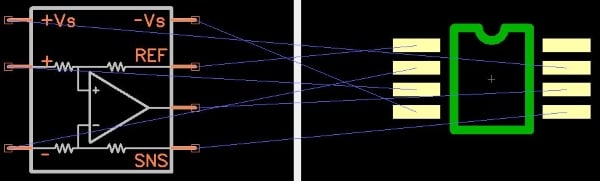
The components include a footprint (AKA land pattern), i.e., a collection of through-holes and/or surface-mount pads that match the terminal geometry of the physical part. A footprint can also have lines, shapes, and text that are collectively referred to as the silkscreen. These show up on the PCB as purely visual elements; they’re not conductive and do not affect the functionality of the circuit.
The following image provides an example of a schematic component and the corresponding PCB footprint (the blue lines indicate the footprint pad to which each component pin is connected).
Converting a Schematic into a PCB Layout
A completed schematic is converted by CAD software into a PCB layout consisting of component footprints and ratlines; this rather unpleasant word refers to electrical connections that have not yet been converted into physical connections.
The designer arranges components and then uses the ratlines as a guide for creating traces, copper pours, and vias. A via is a small through-hole that carries an electrical connection to a different PCB layer (or to multiple layers—e.g., a thermal via might connect to the internal ground plane and a ground-connected copper pour on the bottom of the board).
Verification: Identifying Issues in PCB Layouts
The final step before the beginning of the manufacturing stage is referred to as verification. The general idea here is that the CAD tool attempts to find layout mistakes before they negatively affect the board’s functionality or interfere with the manufacturing process.
I’m familiar with three types of verification (though maybe there are more):
- Connectivity: This ensures that all portions of a net are connected by a conductive structure of some kind.
- Consistency between schematic and layout: This is fairly self-explanatory. I assume that different CAD tools have different ways of implementing this form of verification.
- DRC (design rule check): This one is particularly relevant to the topic of PCB fabrication because design rules are limitations that you impose on your own layout in order to ensure that it can be successfully manufactured. Common design rules include minimum trace spacing, minimum trace width, and minimum drill diameter. It’s easy to violate design rules when you’re laying out a board, especially if you’re in a hurry, so by all means take advantage of the CAD tool’s DRC functionality. The following image conveys the design rules that I used for the C-BISCUIT robot control board.

PCB features are listed horizontally and vertically. The value at the intersection of the row and column corresponding to two features indicates the minimum separation (in mils) between those two features. For example, if you look at the row corresponding to “Board” and then go over to the column corresponding to “Pad,” you see that the minimum separation between a pad and the edge of the board is 11 mils.
Guide to Ordering and Assembling Printed Circuit Boards
This article is part of a series. Check out the rest of the series below:
- PCB Schematic and Board Layout
- How to Generate Manufacturing Files for Custom Printed Circuit Boards
Choosing the Right CAD Software Program: Where to Start
Before we conclude this portion of our guide, I want to briefly discuss schematic/PCB CAD software. If you’re feeling a bit lost amidst the various free and low-cost options, I recommend that you start with one of the following packages:
DipTrace
DipTrace is first on the list because it’s my favorite. The prices are reasonable, it does everything I need it to, and I find the user interface to be intuitive and visually pleasing.
EAGLE
I have very limited experience with EAGLE, but it has been around a long time and it seems to be quite popular. The “standard” license is $100 per year; that’s more than I want to pay for CAD software.
Check out our articles on using EAGLE CAD more effectively below:
- Easier PCB Design: Eagle CAD Tips and Tricks
- EAGLE CAD Tips and Tricks, Part 2
- EAGLE CAD Tips and Tricks, Part 3
- Extend EAGLE CAD Tool with ULPs: Writing Your First User Language Program
KiCad
This program is free and open source. I always avoided it, in part because I was worried about its stability. However, I recently heard from a highly qualified colleague that KiCad has grown into an excellent tool, even for professional designers. It’s definitely worth a look, especially if you’re on a tight budget.
DesignSpark
Completely free and very capable. I used this tool before I switched to DipTrace.
Are there other CAD programs you've used? Tell us about them in the comments below.
The next portion of the custom PCB manufacturing process we'll discuss is how to generate manufacturing files to submit to a fab house.


Mostly windows centric ecad software choices here. Except perhaps for eagle, although kicad has a mac version, I looked at it and wasn’t too impressed. Not many mac options available really…
I use Eagle. The free license is still available though you do need internet access every 15 days to renew it. If you go looking you can still find pre autodesk versions that work perfectly fine still on some p2p platforms. I paid the 100 a year for the multi layers and larger build area at work. At home I still have a V8 copy that is pre autodesk and that works great for me at home.
I also use DipTrace and I am delighted with this program. In particular, it is constantly being developed and has more functionalities. And the price / performance ratio is amazing.