 Facebook
 Google
 GitHub
 Linkedin
Easier PCB Design: EAGLE CAD Tips and Tricks Part 3
More important tips and tricks for using EAGLE CAD to help make your work much easier and faster.
In the previous parts of this series, we learned how to make designing a PCB faster using EAGLE, such as by ripping up all polygons and disabling a bunch of layers using one command. I also brought up some tips about libraries in EAGLE—how to use a reference library, and how to search effectively for a part. Let’s continue talking about other useful tips and tricks in this new article.
Welcome to the EAGLE CAD tips and tricks series!
Check out our other EAGLE CAD articles here:
- Easier PCB Design: EAGLE CAD Tips and Tricks
- EAGLE CAD Tips and Tricks, Part 2
- Extend EAGLE CAD Tool with ULPs: Writing Your First User Language Program
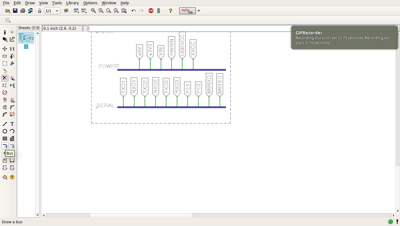
Tip #8: Group Signals into a Bus for Fast Review
Reviewing a colleague's or even your own schematic is a tedious task, especially for complicated designs; lots of wires here and there. This tip will make schematic review go more smoothly.
We will use a tool from EAGLE called ‘Bus’ to gather signals into a logical group. For example, we will gather +5v, +3V3, VIN, PWRIN, USBVCC, and XVCC signals into a bus (logical group) called POWER.
To implement this tip, we need to draw a bus line first, then we name it as the following:
POWER:+5V,+3V3,VIN,PWRIN,USBVCC,XVCC
Using “show” tool with this bus will highlight all signals grouped in this bus both in the schematic and the board.
You can see this tip in action in the following GIF.
Tip #9: Some Signal Names in a Multi-Sheet Schematic Have an Additional Number Added Automatically. Why? How Can We Disable This?
If you have used a multi-sheet schematic in EAGLE before, then you may find some of the signal labels strange, such as MISO_A/2.1E; the original signal name doesn’t have this extra “/X.XX” stuff.
")
Example: Signals with XREF Label (Sheet 1).
This feature is related to XREF type. According to the EAGLE manual, this type of label ("cross-reference" label) is used in multi-sheet schematics to indicate the next sheet a particular signal appears on.

Plain type (left); XREF type (right).
So basically MISO_A/2.1E means that the MISO_A signal also appears on sheet number two, and 1E means that it appears in row 1 and column E (if your schematic is inside a frame).
")
Example: Signals with XREF label (Sheet 2).
To disable this feature, go to Options->Set->Misc->Xref label format, and change it from this format %F%N/%S.%C%R to this one %F%N.
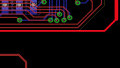
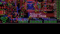
Tip #10: Changing the Distance Between Polygon and Board Dimension
A buffer area is kept between the copper polygon and the board dimensions. In some cases, some areas in the PCB are isolated from the GND polygon, and the only solution is to make this buffer area smaller.

Before changing the buffer value.
To change the value of this buffer area, go to the Design Rule Check (DRC) dialog and then Distance->Copper/Dimension and change that value. Now hit ratsnest again.

After changing the buffer value.
Tip #11: How to Make Package Creation Fast (Really Fast!)
Creating a new package is a time-consuming task for PCB designers. You need to do a lot of calculation while adding PADs/SMDs and lines.
Actually, using grid division can save you time. For example, if you want to create the following footprint you can follow these steps:

3FD-5XX transformer footprint.
- Change grid to 7.62mm. Draw pad 1 and 2.
- Change grid to 10.16mm. Draw pad 3.
- Change grid to 7.62mm. Draw pad 4.
- Change grid to 35.82mm. Copy pads created in the previous steps.
Trick #10: Start Routing with the Same Width as an Existing Wire from Any Point
Our PCB may have many route widths, according to the functionality of the various traces. For example, power traces have widths that differ from data-signal trace widths. I struggle with repeatedly changing the width manually and personally find it an interrupting process, especially when finalizing a PCB design, which involves deleting parts of traces and rerouting them.
Your route can be adapted to the existing route by pressing Shift while routing. The real magic comes when you apply Trick #5 in combination with this trick.
Pressing Ctrl and Shift with a right mouse click causes the trace to start from the pointer position and with the same width as that route.

Trick #11: How to Move a Group for a Set Distance
You can move a group using the mouse, but sometimes you need to move the group for a defined offset, let’s say +50 mil. Ordinarily, we do that by moving each part alone or by using Move: group which is very tricky.
In this trick you need to define a group first using the group tool, then use this command:
MOVE (>0 0) (X_offset Y_offset)
X_offset and Y_offset specify the moving distance. They can be a positive value if you want to move the group right/up or negative if you want to move them left/down.

Trick #12: Enable/Disable Layers as a Group
This trick helps a lot when reviewing a PCB design; you normally need to review the PCB layer by layer (top layers first and then bottom layers).
Instead of performing enable/disable on them one by one, you can group currently enabled layers in an alias. The aliases can be accessed by clicking on the DISPLAY button and holding the mouse button pressed until the list pops up. A right click on the button also pops up the list.

Trick #13: EAGLE Menu Customization
EAGLE CAD loads some configurations during startup from a file called "src/eagle.src". You can add a menu using this script file.

Adding "BOM" menu.
I find this trick useful for quick actions. As an example, I added a button to run the file bom.ulp. You can do that by adding this line under the "SCH:" section:
MENU 'BOM : run bom.ulp;'\
Related Content


I’m not too happy with EagleCAD now that it’s owned by Autodesk, and you have to login. I’m sick and tired of every company thinking it needs it’s nose up my butt all the time.
In fact, i think kicad is the better one.