 Facebook
 Google
 GitHub
 Linkedin
PCB Layout Tips and Tricks: Use a Ground Plane Whenever Possible
This article discusses the importance of proper grounding techniques in PCB design.
This article discusses the importance of proper grounding techniques in PCB design.
Related Information
- Practical PCB Layout Tips Every Designer Needs to Know
- PCB Layout Style Mistakes That Can Ruin Your Design
I don’t deny that it is possible to design a PCB without a ground plane, and in many cases you can create a fully functional board this way (or at least it will be fully functional when operating in a favorable environment). But ground planes are an easy way to improve performance and prevent problems, and in my opinion there are few situations in which it is a good idea to make ground connections using ordinary traces.
Copper Is a Resistor
Schematic diagrams have wires, but in real life there are no wires (unless someone has started manufacturing PCBs using superconductors...). Physical interconnects, including PCB traces, are low-value resistors. The fact that we can often ignore this interconnect resistance doesn’t mean that it has no effect on the functionality of a circuit. On page 8 of this document published by Analog Devices, the author demonstrates that a 5 cm PCB trace can introduce over 1 LSb of error in the digitized values generated by a 16-bit ADC.

AAC’s trace resistance calculator page has more information on the equation shown above.
In many cases there is not much we can do to mitigate the effects of resistance in a signal trace: tiny ICs and the desire for circuit miniaturization often lead to crowded layouts that don’t allow for wide traces or optimal component placement. We can, however, improve the overall situation by using a ground plane, which reduces the resistance of the return path.
This decreased return-path resistance is a fundamental benefit of incorporating a ground plane into your PCB. It reduces noise caused by variations in return current, and it establishes a more uniform ground voltage (because less resistance means less voltage being dropped between physically separated portions of the ground net). By dedicating an entire layer to ground and connecting everything to the plane using vias and through-holes, you are making your physical circuit more like the idealized circuit in the schematic diagram.
Simpler and Smaller
A ground plane improves the electrical characteristics of your circuit while also simplifying your layout task and in some cases reducing the size of your PCB. I’m not going to dwell on these aspects because I think that they’re more or less self-explanatory. The plane allows you to access the ground net anywhere you can squeeze in a via—and squeezing in a via is far easier than snaking a ground connection through a tangled assortment of traces, copper pours, and fine-pitch ICs.
This improved routing may allow you to push the components closer together and thus decrease board size, though there is also the possibility that the board will end up larger if the ground plane causes you to lose one of two component layers (I’ll revisit this issue toward the end of the article).
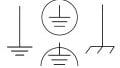
Avoid Ground Loops
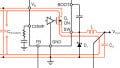
In my experience, the term “ground loop” can refer to any situation in which a system is affected by a difference in ground potential. A typical example is when two modules are connected by a long cable and the return current in the cable causes one module’s ground voltage to be significantly higher than the other module’s ground voltage. In this discussion, though, I’m referring specifically to a loop of ground connections; for example:

If you have to make numerous ground connections using individual PCB traces, it would not be difficult to create a loop like the one shown above. If you’ve read my article on mutual inductance, you know that this sort of conductive loop is a good receiver of magnetic interference.
The presence of a ground plane does not make it impossible to create a ground loop, since the CAD program won’t prevent you from drawing traces between ground points. But if you consistently make your ground connections using vias or through-holes, the problem should largely disappear: by dropping vias to the plane you are making a direct connection from the component to a ground point that is connected through low impedance to all other ground points in the circuit.

An Integrated Shield
A solid ground plane provides some degree of protection against electromagnetic interference (both radiated and received). I wouldn’t rely on a ground plane to solve all of your EMI problems, especially if you have components on both sides of the board; a carefully designed conductive enclosure would be more effective. Nonetheless, every little bit helps, and if you’re concerned about EMI then you have one more reason to incorporate a ground plane into your layout.
The PCB-Plane Capacitor
This is not a major benefit, and it applies only to ground planes that are adjacent to a power plane. I think it’s still worth mentioning, though. A ground plane separated from a power plane by a thin dielectric sounds a lot like a parallel-plate capacitor, and that’s exactly what it is. This structure adds a bit of distributed power-supply capacitance to your entire circuit board, though it certainly isn’t going to replace your decoupling capacitors.
Practical Impediments
I cannot imagine a scenario in which a four-layer PCB would not have a ground plane. I suppose it’s possible that a very dense layout would need both internal layers for normal signal routing, but honestly that seems unlikely: there’s no doubt that the plane occupies routing area, but by simplifying ground connections it also reduces the amount of routing area that the board will require.
A much more realistic scenario is that a ground plane is omitted because schedule or budgetary concerns argue in favor of a two-layer board. Now the ground plane is consuming one of only two PCB layers. Is it really better to include a ground plane if that means cramming almost all of the traces and components onto one layer? In my opinion, yes, it’s still better to include a ground plane, unless the circuit is so straightforward that you can use well-organized, low-impedance traces to make your ground connections. But honestly, if your space constraints are so extreme that you can’t make the board large enough to accommodate a ground layer on the bottom and a clean layout on the top, you should move to a four-layer board.

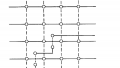
This is the ground layer for a two-layer board that I designed a while ago. Sometimes you really need the second layer as an escape route for a few difficult connections, and that’s not a major problem. The plane layer doesn’t have to be 100% ground.
Summary
Adding a ground plane to your PCB is a simple, low-cost, highly effective way to design electronic devices that have better signal integrity, higher accuracy, and more resistance to interference. If you’re not in the habit of incorporating a ground plane, make sure to keep these benefits in mind when it comes time to lay out your next board.
Related Content


Robert, your section on ground loops is not particularly clear. The illustration may or may not really be a ground loop. It really depends on where the power supply rails are placed and where the signals that use ground as a current return path are placed.
Keep in mind that, for any signal, the return current path from that signal to its source must minimize the area carved out by that path. The best way to layout a signal and its return are next to each other or better yet, one over the other on a multi-layer board, thus minimizing the area of the current from source (the output signal) to load (the input fed from the output signal) and back. The bigger that area the more external EM fields can interfere and the more that signal will radiate. Both are bad side effects.
This applies to power rails (with the power supply being the “output” and the circuit itself being the “input”) as well as signals from one IC to another. Both have a current source and a return path and both must minimize the area inside that path to reduce EM field interference.
You are correct that a ground plane is better. It achieves better results by allowing the current return path to follow the signal path directly adjacent to it on the ground plane. This minimizes the area, as noted above, thus reducing EM interference and unwanted radiated EM fields.
Please include thermal reliefs so I have a chance to get the part off of the lead-free board.