Facebook
 Google
 GitHub
 Linkedin
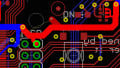
PCB Layout Tips and Tricks: Minimizing Decoupling Inductance
This article examines some subtle details associated with the high-frequency performance of decoupling capacitors.
This article examines some subtle details associated with the high-frequency performance of decoupling capacitors.
Related Information
- Clean Power for Every IC: Understanding Bypass Capacitors
- Clean Power for Every IC: Choosing and Using Your Bypass Capacitors
In the previous article we explored the question of whether to connect a decoupling capacitor to an IC power pin through a trace or through a pair of vias. We saw that the pair-of-vias technique is superior because it reduces inductance, and inductance is the primary obstacle that we have to overcome when we’re trying to ensure that decoupling capacitors will be effective at frequencies of 50–100 MHz and even up into the hundreds of megahertz.
Vias and Planes
In this article we’re going to explore the issue of decoupling-cap inductance as it relates to via and plane-layer configurations. Before we jump into that discussion, though, we need to be clear on the following point: as we go deeper into the realm of high-speed decoupling, we focus more and more on plane connections, until eventually it seems that traces are largely ignored. The following considerations will help to contextualize this phenomenon:
High Inductance
As we saw in the previous article, traces simply have too much inductance compared to connections that rely on vias in conjunction with plane layers.
Plane Capacitance
The way in which the decoupling capacitance interacts with the planes seems to become a dominant factor as operational frequency increases. The science starts to get complicated here, and I have limited ability to understand the details and even less ability to explain them. One interesting and straightforward statement that I found in this article indicates that in some cases the decoupling capacitor itself is so hindered by inductance that it cannot really supply current to the IC. Rather, the plane capacitance supplies the transient decoupling current, and the capacitor’s job is to recharge the planes.
Crowded Layouts
High-speed digital systems often involve complex, space-constrained layouts that dedicate most of the PCB real estate to components. There is little room for traces, and consequently board designers gladly use vias whenever possible.
Distributed Capacitance vs. Discrete Capacitance
If the plane capacitance is the true source of decoupling charge in some high-speed digital designs, does the capacitor really need to be “as close to the pin as possible”? Does the location even matter? It may seem shocking to question the validity of one of the essential principles of proper decoupling, but this is exactly what Hubing et al. did in this research paper. In the words of the authors of this other paper, Hubing et al. claimed that under certain conditions the location of the capacitor is “unimportant,” though they may have extended their conclusions “beyond the region of validity of the study.” In any event, this is another example of the importance of the interaction between the capacitor and the plane layers, which function as “distributed capacitance” present everywhere on the board.
Minimizing Inductance
The overall inductance of a decoupling capacitor depends on the area of the current loop formed by the capacitor, the vias, and the planes.

As you can see, the loop area is influenced by both the separation between the two vias and the distance between the capacitor and the plane layers. Thus, distance to the plane and via separation are critical factors that need to be addressed if the goal is to improve decoupling performance.
Distance to the Plane
If you’re designing a typical four-layer board, there’s not much you can do to reduce the distance to the plane—the decoupling cap will always be close to one plane layer and far from the other.

If the board has more than four layers, though, you have some flexibility in optimizing the location of your decoupling caps relative to the power and ground planes. Also, this is a good time to point out that you’ll lose a lot of distributed capacitance if you don’t place the power and ground planes on adjacent layers. It seems to me that a high-speed digital design would benefit greatly from the following configuration:
- Place as many high-speed ICs as possible on one of the two component layers (let’s say it’s the top).
- Arrange the power and ground planes so that they are adjacent and closer to the top layer.
- Place all the decoupling caps on the top layer so that they have short connections to the planes.
Via Separation
The first way to reduce via separation is to use smaller decoupling caps. On my boards I use 0603 packages because I often assemble them by hand; if the board will be assembled by machines, 0402 is a better choice.
Minimizing inductance is now a matter of choosing the optimal via configuration:

Adapted from the diagram on page 29 of this document.
Notice here that we’re primarily concerned about the distance between the two vias. Thus, the third diagram is labeled “good” and the second is labeled “decent” despite the fact that the “decent” configuration uses shorter traces to connect the capacitor terminals to the vias.
Conclusion
I hope that this article has given you some insight into the complicated world of high-speed digital PCB design. I think it’s pretty clear that minimizing loop area is the key to reducing inductance and hence improving high-frequency performance, but I’m not sure what to think about the possibility (in certain situations) of randomly distributing decoupling capacitors throughout the board. If you have any thoughts on this subject, feel free to share them in a comment.