Facebook
 Google
 GitHub
 Linkedin
Tips and Techniques for DC-DC Buck Converter PCB Layout
Learn best layout practices for your DC-DC buck converter circuits.
Learn best layout practices for your DC-DC buck converter circuits.
In implementing DC-DC buck converters, circuit layout is just as important as design. A great design can be severely degraded by bad layout.
This article will go over some best layout practices.
Goals of Good Circuit Layout
Here are some goals of good layout to keep in mind.
- Control of radiated and induced noise
- Reduced interference between different parts of the circuit
- Reduced circuit area
- Effective thermal management
- Improved voltage regulation and circuit efficiency
- Avoidance of extra “band-aid” circuitry like snubbers
- Enhanced stability
Note: Don’t use autorouting for these critical paths—route and design by hand.
Current Loops in Power Converter Circuits
Power converter circuits generate large currents which, at different phases, circulate in two main loops: off-state and on-state, depending on the state of the MOSFET switch (see Figure 1).

Figure 1(a): On-state current loop; 1(b) Off-state loop. Click to enlarge.
The 3D geometry of these loops is important. Current running in a physical loop, per Ampere’s law, will form a magnetic field in proportion to the current and the loop area. This field can then couple with other circuit loops, per Faraday’s law, with more coupling at higher frequencies, resulting in harmful crosstalk.
Therefore, the general mindset should be to minimize the enclosed area of these loops. A straightforward way to do this is to make the return path as collinear to the outbound path as possible.
Picture a loop antenna squashed down to a vertical line—it will stop being an antenna. This is why we twist wires together to eliminate coupled noise.
Return Paths
Note that a return current, if given an infinite ground plane, will naturally tend to concentrate directly below the outbound current (see Figure 2). We should take this hint from nature and provide the natural return path; otherwise, a loop will be introduced and radiate.
The desired result for the board will be outbound and return currents running in orderly, known paths.

Figure 2: Natural return current paths
Usually, a circuit has multiple ground planes: analog, digital, and power, for example. Although conventional wisdom on this has varied over the years, we shouldn’t need to partition ground planes if these natural return paths are provided. In fact, partitions can make things worse if an unplanned-for return current has to take a long route around it.
Natural current paths in addition to smart partitions may be the best solution.
Rapid-Fire Best Practices
Of course, a key consideration is the location where the power rails enter or originate on the board. If these considerations are under the designer’s control, those should be chosen to promote good layout. Note the same loop philosophy should be applied to the MOSFET gate drive as well because it has large, spiky currents too.
For further control of radiated emissions, the “20H rule” dictates, for layers with spacing of H, that we keep all traces at least 20H from the board edge. It’s usually necessary to push power paths to other layers using power vias to get a tight layout—you just need to manage the effect of those vias like any other element in the power path. The inductance, resistance, and the total number of vias will all affect the path performance.
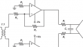
Sensitive control circuits need a clean ground. If we send the large, pulsing power return current through a return path shared by the control, voltage spikes will be created which will perturb the control’s ground, injecting noise into the control circuitry, which is highly undesirable. We use star grounding to avoid this (see Figure 3)—it keeps return paths unshared and separate.
Figure 3: Star grounding
In bypassing supply voltages to ICs, always give proximity priority to the high-frequency components first. Avoid vias and connect directly to IC pins.
Consider the IC manufacturer’s example layout, like an evaluation board, as guidance. However, keep in mind that board might have a stack-up and design goals that are different from yours – for example, achieving the best thermal performance to the detriment of other parameters.
For power traces, the width, length, and thickness must be designed to limit the voltage drop and trace inductance. The voltage drop is more important than ever with the low output voltages of today.
Another main law we need to let guide us is that of capacitive coupling—two plates (circuit nodes) in proximity to each other will couple in proportion to the plate area and the distance between them, with more coupling at higher frequencies and higher recipient node impedance.
For example, voltage feedback is achieved by connecting the sense pin to the output, and this signal should be routed away from noise sources like the switch node and the inductor. The sense pin node is high-impedance and therefore more susceptible to capacitive coupling—keep it as small as possible and isolated from noise sources. Intervening DC planes can reduce coupling as well.
Nodes with high dv/dt transients, like the switch node, need to be kept small and isolated, while still maintaining sufficient current capacity, so they don’t become noise sources.
There will be a necessary sense point placement compromise if there are multiple load points for one power rail—you can put preference on one load or place centrally. If sensing signal is differential, that’s good, but it should be routed like a transmission line. Place any sense circuit resistors near the IC.
How many layers should a board have? More layers mean more room to route and more supply and ground planes that can provide shielding, but also more vias and more cost. For modern converter ICs, you should probably have at least four layers. Also, the number of layers is often not under the power designer’s control, being dictated by other considerations. Generally, the fewer layers you have, the more creative you’ll have to be to get an effective layout.
Thermal Considerations
Layout is also driven by thermal considerations, most obviously by the thermal pad for the IC and the MOSFETs, through which most of the heat is conducted into the board and then radiated into the air. Thermal pad size and number of layers, number of vias, max ambient temperature, and available airflow all need to be considered. Ultimately, an external heatsink may be necessary for the MOSFETs. The datasheet will have at least one thermal example that you can use to guide your thermal design.
Also, be sure to know whether to connect the IC pad electrically or not—it’s not always specified in the datasheet. A nice trick, if you have room, is to extend the pad beyond the edge of the IC on the top layer, giving you a place to heat it to make lifting the IC easier.
Time spent on good layout will more than make up for time spent troubleshooting a badly laid out circuit, and it’s a lot more enjoyable.
Related Content