Facebook
 Google
 GitHub
 Linkedin
PCB Layout Techniques for Reducing Harmonic Distortion of a Differential ADC Driver
Summary
PCB layout is a key factor when optimizing the linearity performance of a high-speed board. The previous articles in this series discussed some basic techniques for reducing the 2nd harmonic distortion. This article, inspired by the TI document “High-Speed PCB Layout Techniques”, attempts to discuss in detail how rail-to-rail and rail-to-ground bypass capacitors should be laid out in high-speed differential ADC drivers to achieve the maximum possible linearity performance.
Differential ADC Drivers Using Single-Ended Op Amps
As shown in Figure 1, a differential ADC driver can be implemented by employing two single-ended op-amps.
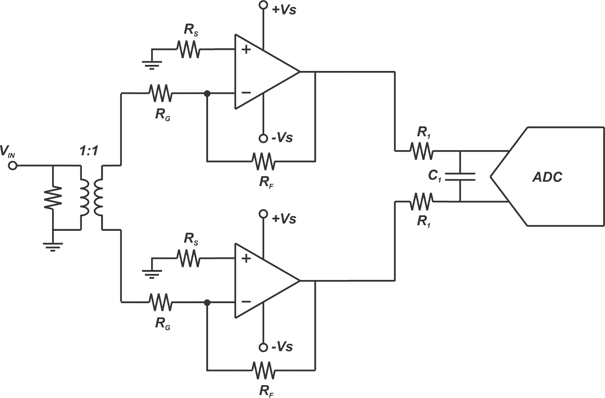
Figure 1. Use of two identical single-ended op-amps to implement a differential ADC driver
With a differential signal applied to these identical paths, the individual op-amps will produce the same 2nd harmonic component. Appearing as a common-mode signal at the ADC input, these distortion components will be suppressed by the differential ADC just like any other common-mode noise and interference signals.
In a previous article, we discussed that a symmetric PCB layout is required to keep the two single-ended paths identical and attenuate the 2nd harmonic. In this article, we’ll discuss how the decoupling capacitors of the op-amps should be laid out to achieve the maximum possible linearity performance.
We know that decoupling capacitors act as sources of charge and provide the high-frequency currents that the op-amps should deliver to the load. To supply the high-frequency differential currents, we can use both rail-to-ground and rail-to-rail decoupling capacitors.
Rail-to-Rail vs Rail-to-Ground Decoupling Structures
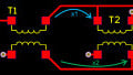
With the structure shown in Figure 1, the current delivered to the load is differential, i.e. when the upper op-amp sources current to the load, the lower branch sinks the current and vice versa. Let’s consider the case where the upper op-amp sources the load current and the lower path sinks it. The rail-to-ground and rail-to-rail decoupling options, as well as the current paths, are shown in Figure 2. Note that in this figure, the resistors of the amplification stages are not shown for simplicity. Besides, we assume that a multi-layer board with a dedicated ground plane is employed.
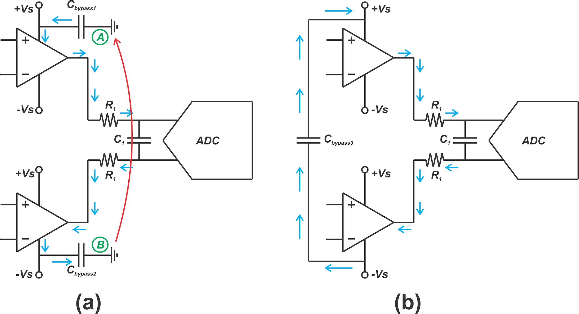
Figure 2. Rail-to-ground (a) and rail-to-rail (b) decoupling structures
With the rail-to-ground decoupling structure (Figure 2(a)), the high-frequency current will flow from the bypass capacitor of the positive rail (Cbypass1) to the load and then, to the bypass capacitor of the negative rail (Cbypass2) as depicted by the blue arrows. The circuit schematic implies that nodes A and B are both at ground level and the path shown by the blue arrows is a closed path of electric current. However, in reality, nodes A and B are two distinct nodes on the ground plane and the current should flow from node B to node A to have a closed current path. Hence, the load current will flow through the path of least impedance provided by the ground plane back to the ground side of Cbypass1.
The challenge with this structure is that any current flowing in the ground plane that is sufficiently close to the load current return path can couple with the load current and alter it. Besides, if the load current return path experiences any asymmetry from node B to A, the symmetry between the single-ended paths of the ADC driver will be affected and a larger 2nd harmonic will appear at the ADC input.
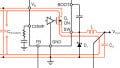
To circumvent these problems, the decoupling structure in Figure 2(b) can be employed where a bypass capacitor is placed between the two rails. In this way, the differential load current will follow the path shown by the blue arrows and it won’t have to flow through the ground plane. According to the TI document, a rail-to-rail bypass capacitor can reduce the 2nd harmonic distortion by 6 to 10dB. Note that, in order to provide the differential load current in the opposite direction, we need to include another rail-to-rail bypass capacitor (Cbypass4) as depicted below in Figure 3.
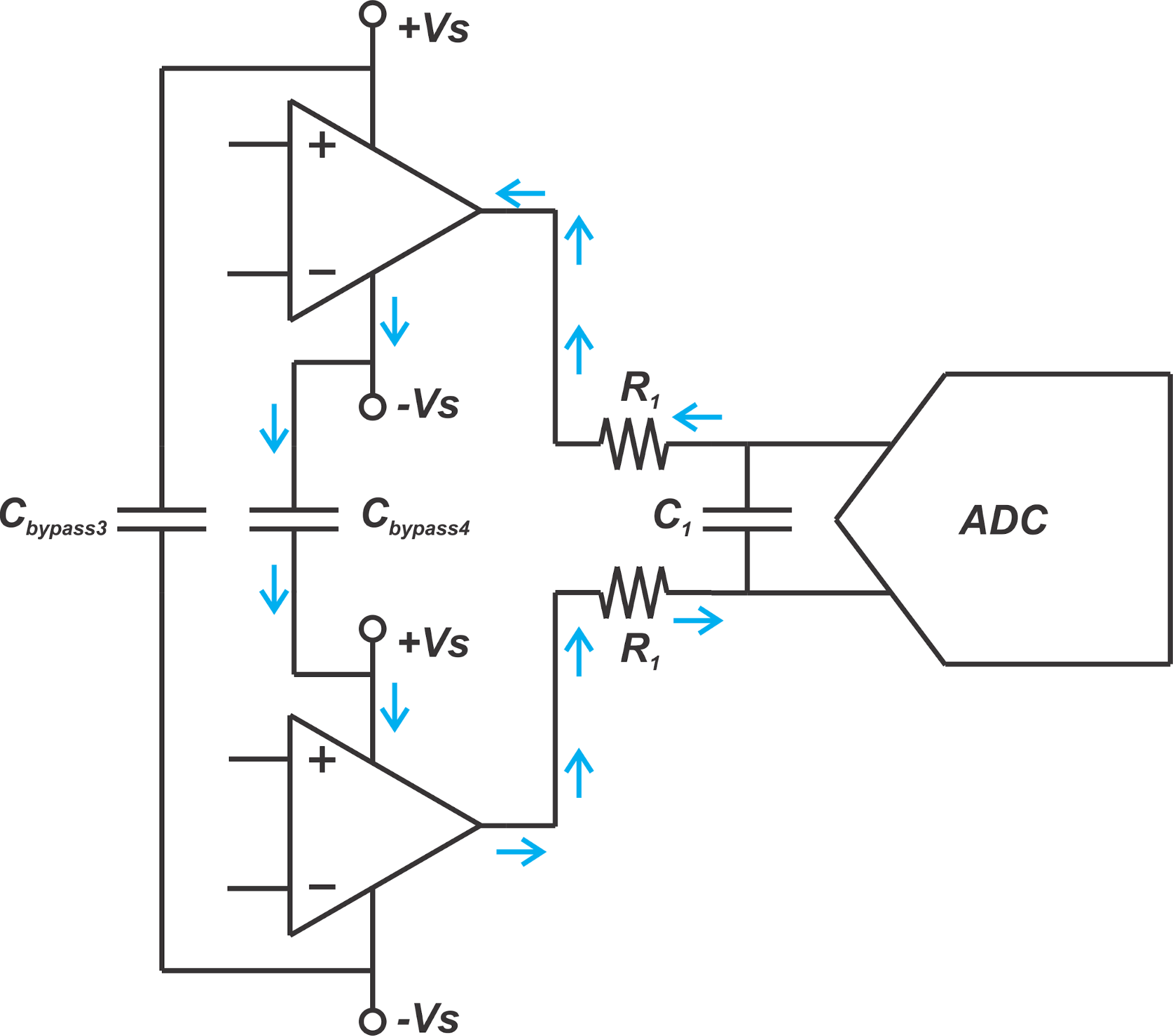
Figure 3
The path for the load current provided by Cbypass4 is shown by the blue arrows.
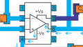
What About Common-Mode Currents?
With the structure depicted in Figure 1, the current provided by the op-amps is mainly differential and can be supplied by the rail-to-rail decoupling capacitors. However, we can still have small common-mode current components. For example, assume that a noise component couples to the non-inverting input of the two op-amps and raises the voltage of these nodes slightly. This will produce a common-mode current flowing out of the two op-amps. As shown in Figure 4, such a common-mode current will charge the stray capacitance of the PCB traces.
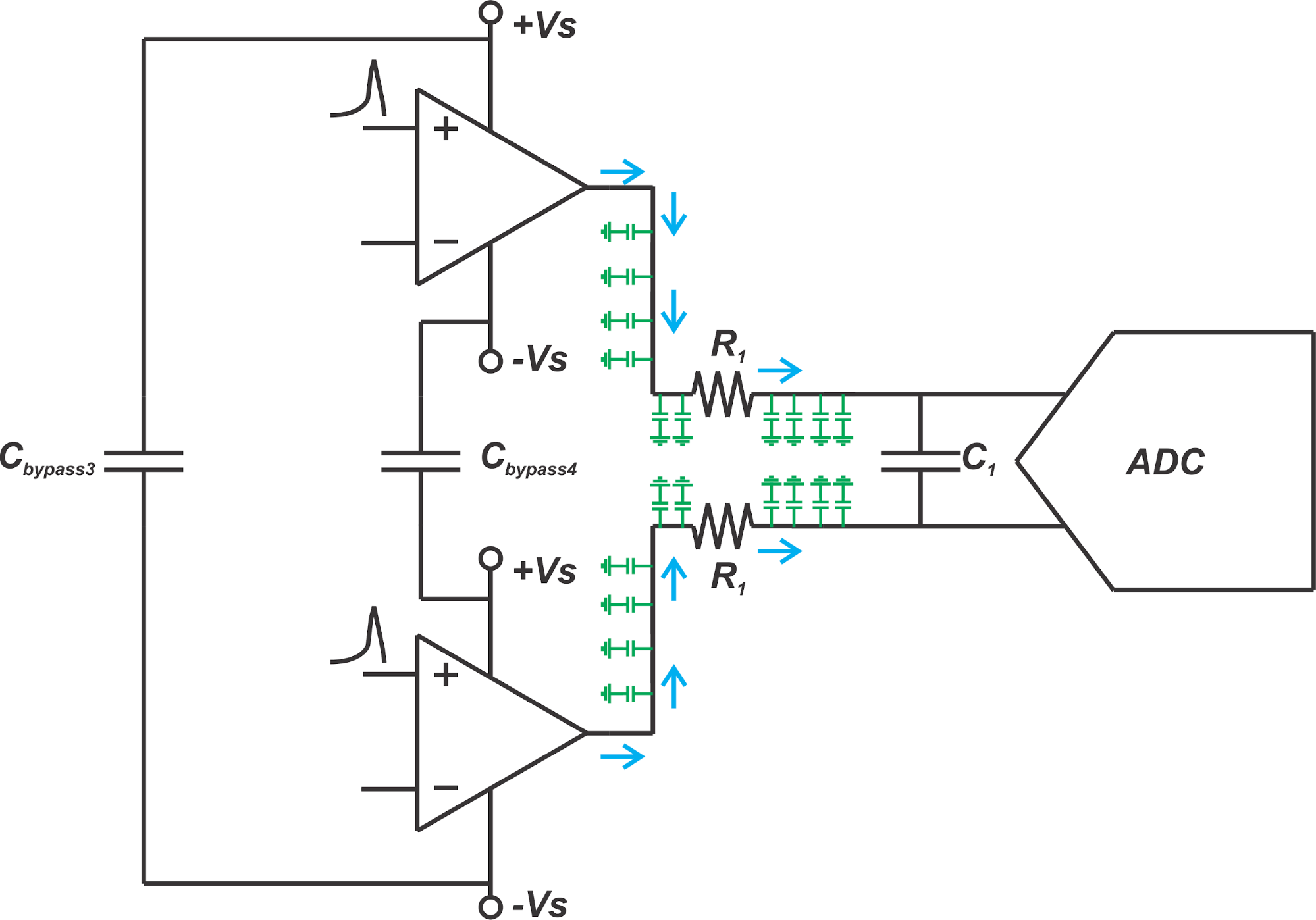
Figure 4
Note that the rail-to-rail bypass capacitors cannot supply these common-mode currents. In Figure 4, the op-amps will have to provide high-frequency common-mode current components directly through the power and ground conductors, which is not desired. Hence, we need to add rail-to-ground bypass capacitors as shown in Figure 5.
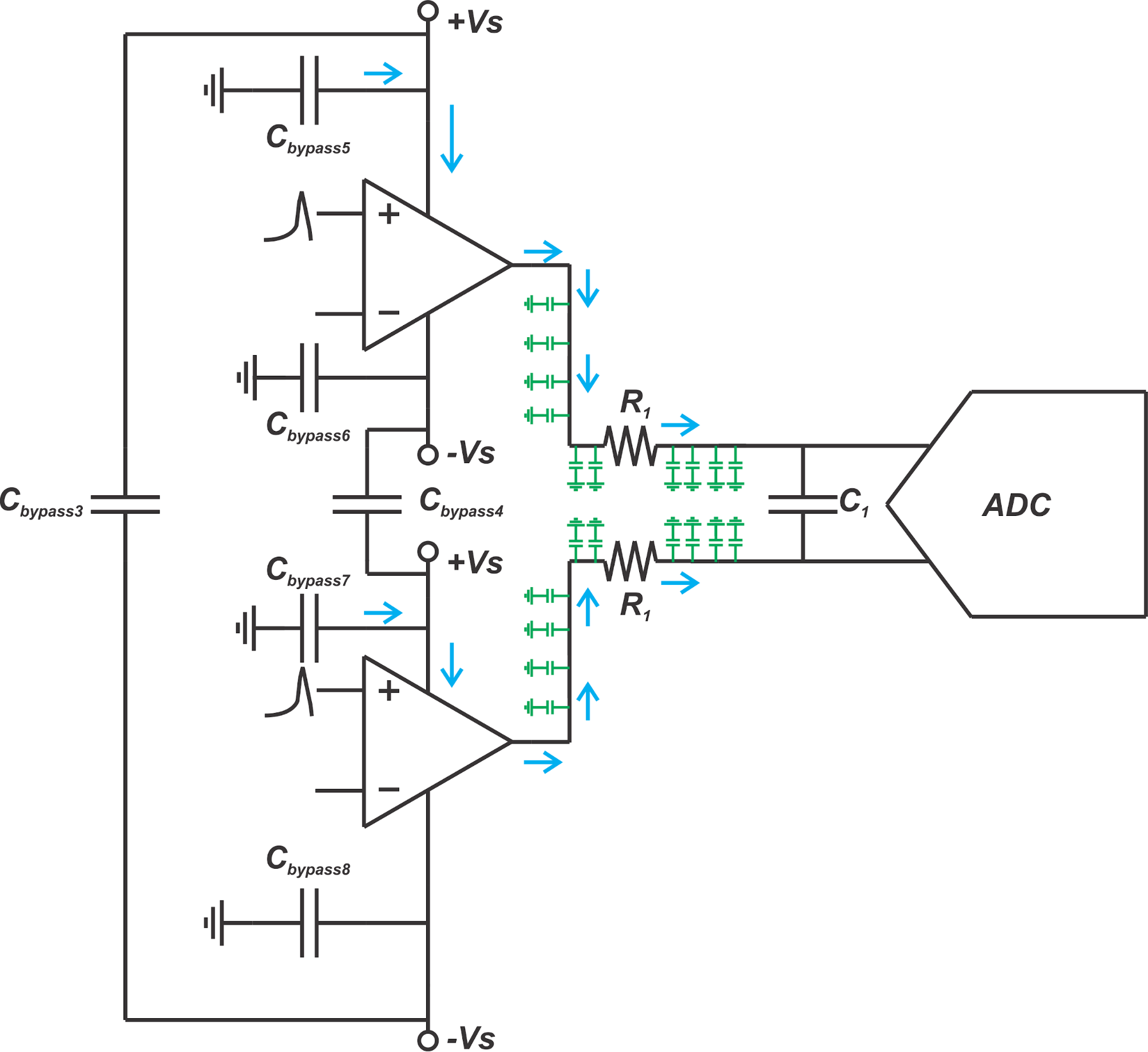
Figure 5
As you can see, the common-mode current flowing out of the two op-amps will be provided by the bypass capacitors between the positive rail and ground (Cbypass5 and Cbypass7). This common-mode current will charge the parasitic capacitance of the traces. Hence, a return current will flow from the ground side of the parasitic capacitances back to the ground side of Cbypass5 and Cbypass7 in the ground plane. Similarly, the common-mode current sunk by the two op-amps will be provided by the bypass capacitors placed between the negative rail and ground (Cbypass6 and Cbypass8).
Rail-to-Ground Caps Can Provide Both Common-Mode and Differential Currents
While we added Cbypass5, Cbypass6, Cbypass7, and Cbypass8 to provide the common-mode currents, these capacitors will also provide a portion of the high-frequency differential current of the load. As illustrated in Figure 2(a), the use of rail-to-ground capacitors can unnecessarily make the differential load current flow through the ground plane which is not desired. To avoid this, we can place the rail-to-ground bypass capacitors that can supply differential currents in a symmetric fashion and ground the trace between them at the midpoint. This is best illustrated graphically in Figure 6.
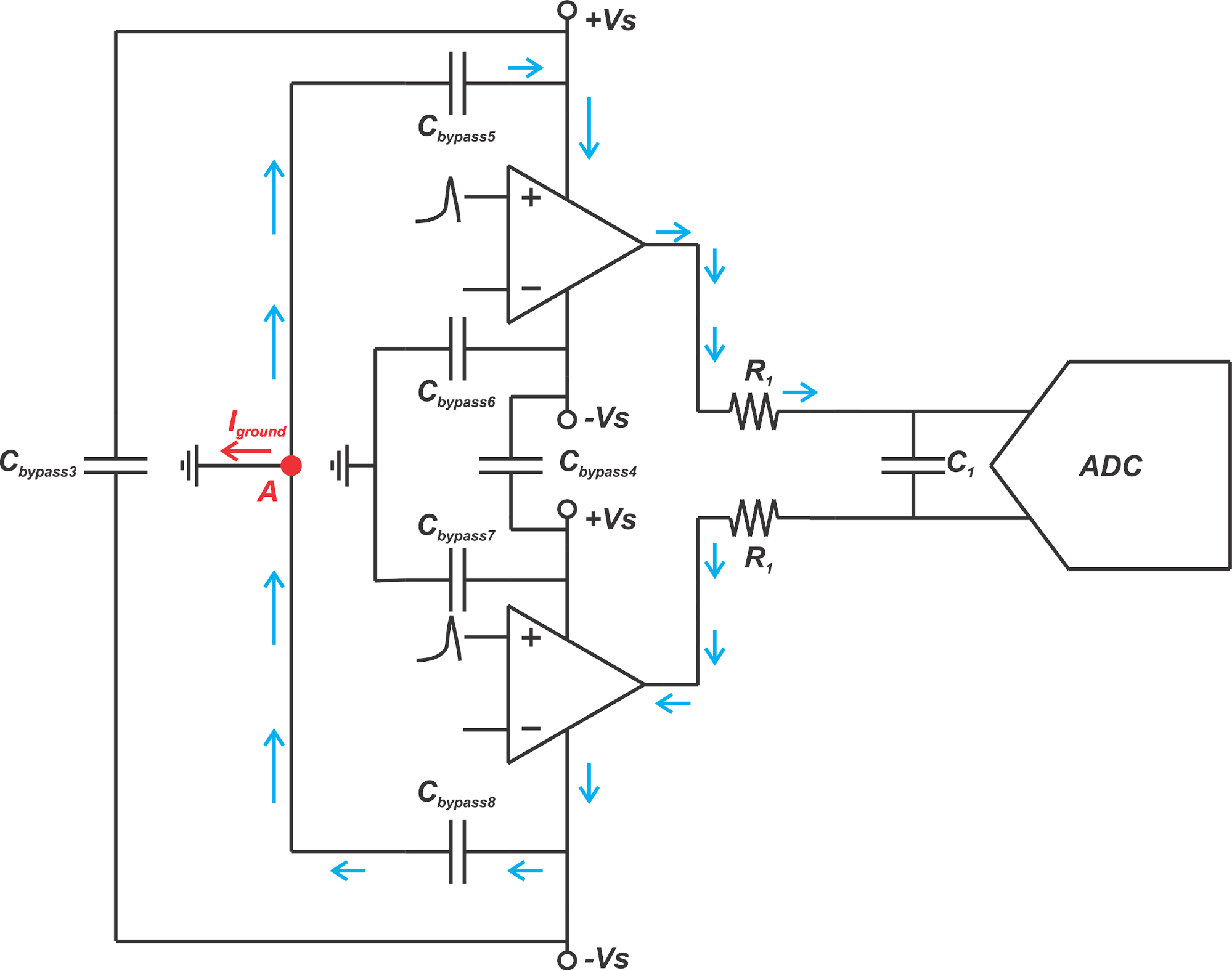
Figure 6
The above figure shows the case where the upper op-amp sources the load current and the lower path sinks it. In this case, Cbypass5 and Cbypass8 can supply a portion of the load differential current. To prevent the differential current from flowing through the ground plane, we connect the ground side of Cbypass5 and Cbypass8 together by a PCB trace on the signal layer of the board and ground this trace at a midpoint (node A in the figure). With a differential signal, node A should be theoretically a virtual ground and the differential current should not flow into the ground plane (Iground=0 for a differential load current). Similarly, we place Cbypass6 and Cbypass7 symmetrically to each other and ground the trace between the two capacitors at the midpoint. You can find an example layout applying the above techniques in this TI application report.
As a final note, it is worthwhile to mention that these techniques are also applicable to ADC drivers based on fully differential op-amps. For more information, please refer to the TI document I mentioned above.
Conclusion
To extract the maximum linearity performance from a differential ADC driver, we need a symmetric PCB layout. Employing a rail-to-rail bypass capacitor as the main charge source for high-frequency differential currents can reduce the 2nd harmonic component by 6 to 10dB. We’ll still need rail-to-ground bypass capacitors to supply the common-mode currents. Since these capacitors can also provide a portion of the load differential current, we need to lay them out symmetrically so that the differential load current cannot flow into the ground plane.