 Facebook
 Google
 GitHub
 Linkedin
Reducing Second Harmonic Distortion with Symmetrical PCB Layout
Need a low-distortion ADC interface? In this article, we'll discuss how to reduce 2nd harmonic distortion by using symmetric PCB layout.
A differential circuit driven by a differential signal produces no even harmonics. In this article, we’ll discuss that to reduce the second harmonic distortion, it is necessary to employ a symmetric PCB layout. Even seemingly slight deviations from a symmetric layout can raise the amplitude of the second harmonic by several decibels.
We’ll also discuss that it is the signal path symmetry rather than the component symmetry that actually determines the even-order distortion performance of the design.
The Basic Technique to Attenuate the Second Harmonic
Driving a symmetric structure by a differential signal is usually the basic technique to suppress the 2nd harmonic. Let’s see how this technique works.
Assume that our nonlinear circuit is memoryless (i.e., the output at any time depends only on the input at the same time). We can use the following equation to approximate the non-linear input-output characteristic:
\[v_{out}(t)=\alpha_1 v_{in}(t)+\alpha_2{v_{in}}^2(t)+\alpha_3{v_{in}}^3(t)+\alpha_4{v_{in}}^4(t)+...\]
where \(v_{in}(t)\) and \(v_{out}(t)\) are the circuit input and output signals, respectively.
In this equation, the coefficient \(\alpha_1\) specifies the linear gain of the circuit and \(\alpha_2\) characterizes the second harmonic distortion. For the sake of analyzing the second harmonic, we can ignore higher order distortion coefficients \((\alpha_3, \alpha_4,\cdots )\) and obtain the simplified equation below:
\[v_{out}(t)=\alpha_1v_{in}(t)+\alpha_2{v_{in}}^2(t)\]
If we employ two replicas of this circuit, one excited with the input \(v_{in}(t)\) and the other one with \(-v_{in}(t)\), we’ll obtain the following outputs:
\[v_{out,+}(t)=\alpha_1v_{in}(t)+\alpha_2{v_{in}}^2(t)\]
\[v_{out,-}(t)=\alpha_1(-v_{in}(t))+\alpha_2(-{v_{in}}(t))^2 = -\alpha_1v_{in}(t)+ \alpha_2{v_{in}}^2(t)\]
Subtracting these two outputs, we have:
\[v_{out,+}(t)-v_{out,-}(t)=2\alpha_1v_{in}(t)\]
While the individual circuits produce the second harmonic, the differential output ideally suppresses the distortion component. This is a very important property of differential operation and explains why a differential circuit driven by a differential signal produces no even harmonics.
In practice, a differential circuit might not completely suppress the even harmonics. However, the even-order harmonics of a differential structure are generally negligible compared to its odd-order harmonics.
Example: A Differential ADC Interface Can Reduce the 2nd Harmonic
The following figure shows an example application where two single-ended signal paths are used to create a differential interface to the ADS5500, a 14-bit, 125-MSPS analog-to-digital converter from TI.
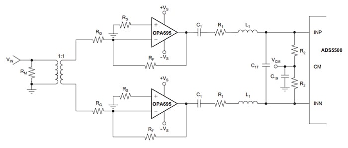
Figure 1, Image courtesy of TI.
The transformer converts the single-ended input to a differential signal. After the transformer, the two signal paths are exactly the same.
It is worthwhile to mention that, in practice, the transformer outputs are not ideal differential signals—phase and/or magnitude imbalance might exist between the two outputs. These imbalances can increase the second harmonic distortion. It can be shown that the second-harmonic amplitude is more severely affected by phase imbalance than by the magnitude imbalance.
Layout Symmetry Is Central to 2nd Harmonic Suppression
In addition to using identical components in the two signal paths, we also need to employ a symmetric PCB layout to maximize the second harmonic cancellation. A non-symmetric layout will prevent us from taking full advantage of the linearity of the active analog blocks, such as ADCs and op-amps, in the signal chain.
As an example, consider the ADC interface shown below.
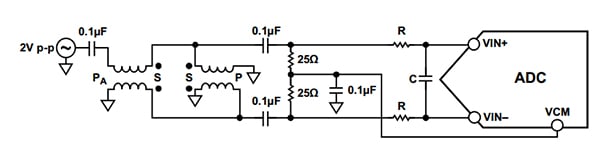
Figure 2. The ADC interface of the AD9266 ADC. Image courtesy of Analog Devices.
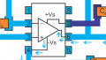
This ADC interface uses the double-balun configuration (depicted below) to convert the single-ended input to a differential signal.
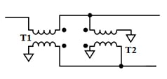
Figure 3. Double balun topology for the single-ended to differential conversion.
This is a common circuit topology for applications where SNR is a key parameter. The double-balun configuration can reduce the phase and magnitude imbalance between the differential outputs compared to a structure that uses only a single balun. The AD9266 (a16-bit, 1.8 V ADC from Analog Devices) datasheet recommends a double-balun structure for frequencies greater than about 10 MHz.
Careful attention should be paid to the layout of this stage to minimize the second harmonic distortion.
Example Layouts for a Double-Balun Structure
Two possible layouts for a double-balun structure are shown in Figures 4 and 5.
Figure 4 is not an ideal layout because the traces running from T1 to T2 are not the same for the upper and lower signal paths (i.e., x1 and x2 are not identical).
Another issue with this layout is that the two grounded pads of T2 are not symmetric.
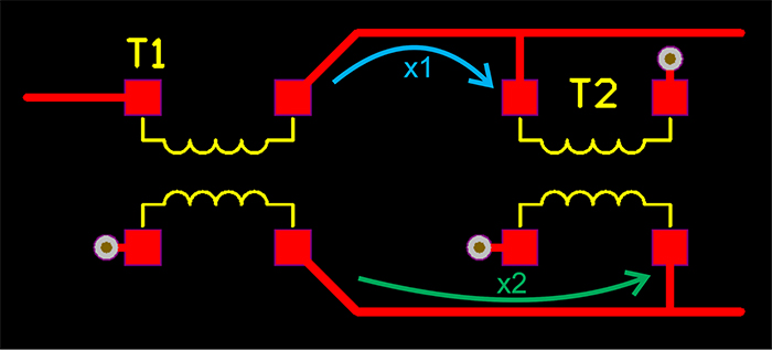
Figure 4. A non-symmetric layout for the double-balun configuration.
Figure 5 shows an alternative layout for this circuit. In this case, the traces connecting T1 to T2 run to a midpoint (n1 for the upper path and n2 for the lower one) and then connect to the corresponding pad of T2. This makes the two paths identical. Additionally, note that a symmetrical trace is used for the two grounded pads of T2.
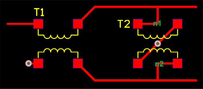
Figure 5. A symmetric layout.
While these adjustments might seem subtle, they can have a remarkable effect on a design's distortion performance. The symmetric layout of Figure 5 can reduce the second harmonic magnitude by about 5dB compared to the layout shown in Figure 4.
Component Symmetry Vs Signal Path Symmetry
To have a symmetric layout, we can sometimes start with placing the components according to a line of symmetry. For example, the resistors and capacitors in Figure 2 above can be placed as in Figure 6.
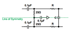
Figure 6
With two-terminal components such as resistors and capacitors, the symmetric component placement should lead to a symmetric layout.
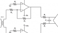
However, this is not the case with non-symmetric packages. For example, consider an op-amp in an SOIC-8 package. As shown in Figure 7, placing two of these packages with respect to a line of symmetry will not create a symmetric layout. In this example, the inverting input of the upper op-amp is further away from the line of symmetry compared to the inverting input of the lower op-amp. In other words, d1 > d2.
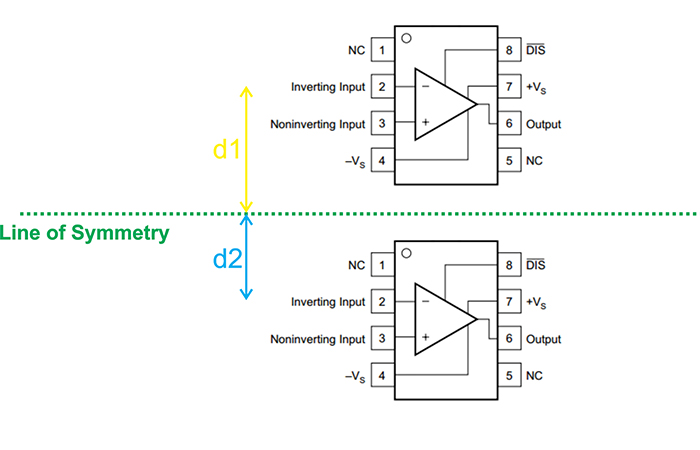
Figure 7
In these cases, we’ll have to consider different lines of symmetry along the signal flow path so that the signal symmetry is preserved.
Consider the figure below:
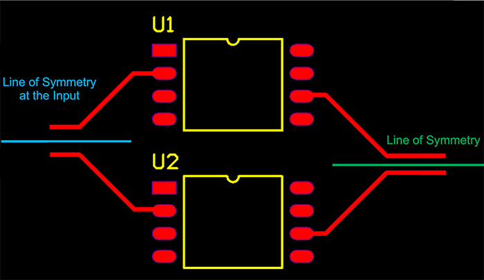
Figure 8
The following figure shows how changing the line of symmetry allows us to maintain the signal path symmetry for the traces running into the op-amp inverting inputs and those at the op-amp outputs.
Conclusion: Key Takeaways for Symmetric Design in Reducing Second Harmonic Distortion
As we established in the introduction of this article, a differential circuit driven by a differential signal produces no even harmonics. To reduce the second harmonic distortion, we need to employ a symmetric PCB layout. Even seemingly subtle deviations from a symmetric layout can raise the amplitude of the second harmonic by several decibels. It should be noted that it is the signal path symmetry rather than the component symmetry that actually determines the even-order distortion performance of the design.
Related Content


In figure 1, shouldn’t the input transformer have a grounded center-tap on its secondary to provide a current path for the op-amp inverting inputs and to truly balance the circuit?