Facebook
 Google
 GitHub
 Linkedin
Designing an Inverse Class F Amplifier With Second-Harmonic Peaking
We explore the implementation and design equations of the second-harmonic peaking amplifier.
In an inverse Class F amplifier, the collector voltage is shaped into a half-sine wave and the collector current takes the form of a square wave. Figure 1 shows the circuit schematic for a basic inverse Class F amplifier.

Figure 1. Circuit diagram of the second-harmonic peaking amplifier.
As we know from the previous article in this series, this configuration is referred to as the second-harmonic peaking amplifier. When we discussed it, however, we mostly focused on the waveforms it produced. In this article, we’ll examine the circuit itself most closely. We’ll then formulate the second-harmonic peaking amplifier’s essential design equations and use them to work through an example.
Operation of the Second-Harmonic Peaking Amplifier
As the previous article noted, the schematic in Figure 1 is almost identical to the schematic for a third-harmonic peaking Class F amplifier. The only difference is that the L2-C2 resonant circuit is tuned to the second harmonic rather than the third.
Together, the L2 and C2 components approximate an open circuit at the second harmonic. However, they behave like a short circuit at other harmonic frequencies. Similarly, the fundamental harmonic resonator (L0 and C0) acts as an open circuit at the fundamental frequency while effectively grounding the output at all other harmonics.
Figure 2 provides a summary of the load network’s impedance at the various harmonics.
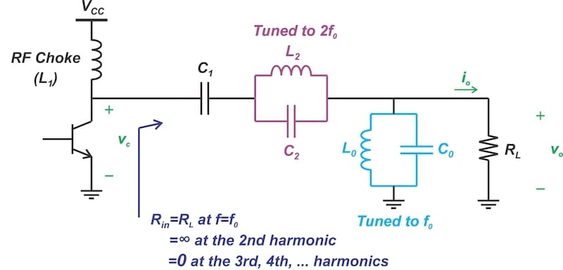
Figure 2. Impedance presented by the amplifier’s load network at different harmonics.
Let’s expand on this summary a bit:
- At the fundamental frequency, the L2-C2 resonant circuit functions as a short circuit and the L0-C0 connection approximates an open circuit. Therefore, at the fundamental frequency, the load network presents an impedance of RL to the transistor.
- At the second harmonic, the L2-C2 connection acts as an open circuit. The collector therefore sees an open circuit.
- At harmonic frequencies beyond the second, both resonant circuits act as short circuits. As a result, the load network effectively presents a short circuit to the transistor.
The voltage across RL is a sinusoidal waveform because the L0-C0 tank short-circuits all but the fundamental current component. The voltage across the L2-C2 tank is a sinusoidal signal at the second harmonic because the L2-C2 connection presents a high impedance to the output current at that frequency. Since the collector voltage is the sum of the load (RL) voltage and the voltage across the L2-C2 tank circuit, a second-harmonic component is added to it.
Collector Voltage and Current Waveforms
The target waveforms of an inverse Class F amplifier are shown in Figure 3.

Figure 3. The collector voltage (top) and current (bottom) waveforms in an ideal inverse Class F amplifier.
As we see above, the collector current is a square wave. To produce this waveform, a second-harmonic peaking stage requires a square wave drive signal.
Meanwhile, the target collector voltage waveform is a half-sinusoid. Because it incorporates only the second harmonic, the collector voltage generated by the second harmonic-peaking amplifier can only approximate this. The collector voltage can be expressed by:
$$v_{F} ~=~ V_{cc} -A_1 \cos(\omega_0 t)~+~A_2 \cos(2 \omega_0 t)$$
Equation 1.
For maximally flat waveforms, the fundamental and second harmonics should satisfy the following conditions:
$$A_1 ~=~ \frac{4}{3} V_{cc} \quad \text{and} \quad A_2~=~\frac{1}{3} V_{cc}$$
Equation 2.
Figure 4 plots the maximally flat collector voltage waveform for a second-harmonic peaking amplifier.

Figure 4. The maximally flat collector voltage for the second-harmonic peaking amplifier is shown in blue.
The minimum collector voltage for a second-harmonic peaking amplifier is ground. However, the maximally flat voltage waveform can reach a peak value of:
$$V_{c,max}~=~\frac{8}{3}V_{cc}~\approx~2.67V_{cc}$$
Equation 3.
Calculating the Output Power
Now that we've determined the amplitude of the fundamental voltage component, let's calculate the average power delivered to the load:
$$P_L~=~ \frac{(v_{o, rms})^2}{R_L}~=~ \frac{1}{2}\frac{ A_1^2}{R_L} \quad \rightarrow \quad P_L ~=~ \frac{8}{9} ~\times~ \frac{V_{cc}^2}{R_L}$$
Equation 4.
That’s about 78% greater than the output power of a Class B stage, which is given by:
$$P_L ~=~ \frac{1}{2} ~\times~ \frac{V_{cc}^2}{R_L}$$
Equation 5.
Calculating the Amplifier’s Efficiency
To calculate the efficiency of the amplifier, we need to determine both the output power (PL from Equation 4) and the power drawn from the supply (Pcc). To compute the power provided by the supply, we find the average value of the current drawn from the supply (Ic, ave) and multiply it by the supply voltage:
$$P_{cc} ~=~ V_{cc} I_{c,ave}$$
Equation 6.
As illustrated by Figure 3, the collector current is a square wave switching between 0 and Icp. By employing the Fourier series representation, the square-wave current through the transistor can be expressed as the sum of its frequency components:
$$i_c ~=~ \frac{I_{cp}}{2}~-~\frac{2I_{cp}}{\pi} \cos(\omega_0 t)~+~\frac{2I_{cp}}{3 \pi} \cos(3 \omega_0 t)~-~\frac{2I_{cp}}{5 \pi} \cos(5 \omega_0 t)~+~...$$
Equation 7.
The Fourier series representation of the signal shows that the DC current drawn from the supply is 0.5Icp. Therefore, Equation 6 produces:
$$P_{cc} ~=~ V_{cc} I_{c,ave}~=~ \frac{ V_{cc} I_{cp}}{2}$$
Equation 8.
We can apply Equations 4 and 8 to determine the amplifier's efficiency, but only once we’ve established a relationship between Icp and Vcc. From Equation 7, we observe that the amplitude of the fundamental component is 2Icp/π. This current passes through the load (RL), resulting in a fundamental voltage amplitude of A1 = 4Vcc/3. From this, we deduce the following:
$$\frac{2I_{cp}}{\pi} ~\times~ R_L ~=~\frac{4}{3} V_{cc} \quad \rightarrow \quad I_{cp} ~=~ \frac{2\pi}{3} ~\times~ \frac{V_{cc}}{R_L}$$
Equation 9.
Combining Equations 8 and 9, the power supplied to the amplifier is:
$$P_{cc} ~=~ \frac{\pi}{3} ~\times~ \frac{V_{cc}^2}{R_L}$$
Equation 10.
Finally, we use Equations 4 and 10 to calculate the efficiency:
$$\eta ~=~ \frac{P_L}{P_{CC}} ~=~ \frac{\frac{8}{9} ~\times~ \frac{V_{cc}^2}{R_L}}{\frac{\pi}{3} ~\times~ \frac{V_{cc}^2}{ R_L}}~=~\frac{8 }{3 \pi}~=~84.9 \ \%$$
Equation 11.
It's important to note that neither efficiency nor output power provide a complete assessment of a power amplifier's performance. For example, the peak collector voltage in a Class B stage is 2Vcc. In the inverse Class F stage we’ve been examining, it’s 2.67Vcc. This means that the high output power of the second-harmonic peaking amplifier is achieved at the cost of greater voltage stress on the transistor.
Output Power Capability
To assess the output power while accounting for the voltage and current stresses on the transistor, we use a parameter called output power capability. For a power amplifier, this parameter is defined as:
$$C_p ~=~ \frac{P_{L, max}}{N I_{c, max}V_{c, max}}$$
Equation 12.
where:
PL,max is the maximum output power
Ic,max is the maximum collector current
Vc,max is the maximum collector voltage
N is the number of transistors in the amplifier.
The output power capability is the output power produced when the device has a peak collector voltage of 1 V and a peak collector current of 1 A. Noting that the output power is equal to Pcc multiplied by the efficiency (η), we can rewrite Equation 12 as:
$$C_p ~=~ \frac{P_{L, max}}{N I_{c, max}V_{c, max}}~=~ \frac{\eta P_{cc}}{N I_{c, max}V_{c, max}}~=~\frac{\eta}{N} ~\times~ \frac{ I_{c,ave}}{I_{c, max}} ~\times~ \frac{V_{cc}}{ V_{c, max}}$$
Equation 13.
As we saw in Equation 3, the maximally flat voltage waveform for a second-harmonic peaking amplifier has a peak value of 8Vcc/3. We also know from Equation 7 that the ratio of the average collector current to its maximum value is 0.5. Substituting these values into Equation 13, we obtain:
$$C_p ~=~ \frac{\eta}{N} ~\times~ \frac{ I_{c,ave}}{I_{c, max}} ~\times~ \frac{V_{cc}}{ V_{c, max}}~=~ \frac{\frac{8}{3\pi}}{1} ~\times~ \frac{1}{2} ~\times~ \frac{V_{cc}}{ \frac{8}{3} V_{cc}} \quad \rightarrow \quad C_p ~=~0.159$$
Equation 14.
By comparison, the output power capability of a Class B stage is Cp = 0.125. This shows that an inverse Class F stage provides a higher output power for the same transistor specifications.
Example: Designing a Second-Harmonic Peaking Amplifier
Say that we’re designing an inverse Class F amplifier with second-harmonic peaking and maximally flat collector voltage. If the supply voltage is Vcc = 30 V, determine the following:
- The load resistance (RL) for an output power of PL = 50 W if the supply voltage is 30 V.
- The maximum current and voltage that the transistor must tolerate.
Let’s start with the load resistance. Substituting the given output power and supply voltage values into Equation 4, we have:
$$P_L ~=~ \frac{8}{9} ~\times~ \frac{V_{cc}^2}{R_L} \quad \rightarrow \quad 50~=~\frac{8}{9} ~\times~ \frac{30^2}{R_L}$$
Equation 15.
which produces RL = 16 Ω.
As we know from Equation 3, the maximum collector voltage in this type of amplifier is:
$$V_{c,max} ~=~ \frac{8}{3} ~\times~ V_{cc} ~=~ \frac{8}{3} ~\times~ 30~=~80 ~\text{V}$$
Equation 16.
Finally, from Equation 9, the maximum collector current is given by:
$$I_{cp} ~=~ \frac{2\pi}{3} ~\times~ \frac{V_{cc}}{R_L}~=~\frac{2\pi}{3} ~\times~ \frac{30}{16} ~=~ 3.93 ~\text{A}$$
Equation 17.
Wrapping Up
The second-harmonic peaking amplifier is a basic inverse Class F configuration that produces an approximately half-sinusoidal collector voltage by incorporating a second-harmonic component. To produce a maximally flat collector voltage waveform, the amplitude of the second harmonic should be one-fourth that of the fundamental frequency component. This leads to an efficiency of η = 84.9%.
This article concludes not only our discussion of inverse Class F amplifiers but also my series on the different power amplifier classes. A complete list of articles in this series is provided below.
Classes A through C:
Class D:
Class E:
Class F and Inverse Class F:
All images used courtesy of Steve Arar
Related Content