Facebook
 Google
 GitHub
 Linkedin
Understanding Switching Losses in Class E Amplifiers
In this article, we examine how non-zero switch transition times impact the efficiency of a Class E power amplifier.
A Class E stage with ideal components is commonly assumed to have an efficiency of 100%. In practice, there are several non-idealities that degrade the efficiency of a Class E amplifier. In this article, we’ll discuss just one: the non-zero transition times of practical switches. Understanding this loss mechanism can help us to more realistically estimate the amplifier’s performance and enable a more accurate thermal system design.
If you’ve been following this article series since “Introduction to the Class E Power Amplifier,” you may recall that the load networks of these amplifiers are designed to minimize switching losses. Even with a non-ideal transistor, the turn-ON switching loss of a well-designed Class E stage can be close to zero. However, the turn-OFF switching loss can be considerable, as we’ll soon see.
Because turn-OFF transitions are when the significant switching losses occur, we’ll spend most of the article discussing them. Before we jump in, though, let’s briefly review the turn-ON transitions.
Losses Due to Non-Zero Rise Time
Figure 1 shows typical switch waveforms for a Class E power amplifier.

Figure 1. Typical switch current (top) and voltage (bottom) waveforms in a Class E amplifier.
Just before the transistor turns ON (for example, at ⍵t = 2π), the voltage across the switch (Vsw) returns to 0 V. The voltage waveform also has a slope of zero (dVsw/dt = 0) at this moment in time. With the zero-voltage switching and zero-derivative switching conditions satisfied, the switch current rises smoothly from zero at the turn-ON time. As a result, both the voltage across the switch and the current through it are very small during the OFF-to-ON transition, resulting in negligible power loss.
Losses Due to Non-Zero Fall Time
Next, let’s examine the power loss during the ON-to-OFF transition. In Figure 1, the switch turns OFF at around ⍵t = π. The current waveform shows the switch current changing instantaneously from ioff to zero when this occurs. For an ideal Class E amplifier, ioff is twice the DC current provided by the power supply (I0). We can easily verify this using the analysis in “Unraveling the Design Equations of the Class E Amplifier.”
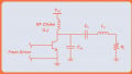
Figure 2 shows the amplifier when the transistor turns OFF. I0 is labeled in green.

Figure 2. When the transistor turns OFF, the current through it is twice I0, the DC current provided by the supply.
To recap, the ideal operation of this amplifier requires a switch that can instantaneously cut off a large current of 2I0. Since a practical switch needs some time to cut off the current, it follows that we won’t achieve ideal operation. Instead of the waveforms in Figure 1, we get the waveforms in Figure 3.
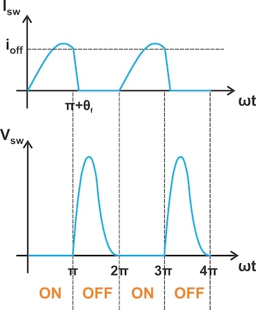
Figure 3. Switch waveforms that account for a non-zero turn-OFF transition.
Here, the non-zero turn-OFF time of the switch causes overlap between the current and voltage waveforms. The IV product is therefore greater than zero during those intervals, leading to power loss during the ON-to-OFF transitions.
In the next section, we’ll use the approximate waveforms in Figure 3 to calculate the turn-OFF switching loss. Before we move on, note that the above figure assumes that the current reduces linearly from ioff at ⍵t = π to 0 at ⍵t = π + θf. Though more precise, sophisticated models exist in scholarly works, the linear model suffices for us to develop a basic understanding of the circuit’s behavior.
Calculating the Turn-OFF Power Loss
Figure 4 shows one period of the switch waveforms for our analysis. To simplify our equations, the time origin has been changed to the instant when switch turn-OFF is triggered.
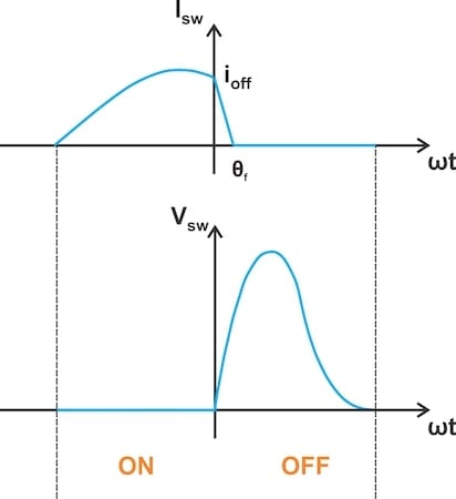
Figure 4. Switch waveforms for use in the power loss analysis.
To calculate the turn-OFF switching loss, we first determine the current flowing through the switch and the voltage across it. Then, we compute the integral of the product of the switch's voltage (Vsw) and current (Isw) over the duration of the turn-OFF transition.
Based on the linear model of current variation, the switch current equation is:
$$i_{sw} ~=~ i_{off}(1~-~ \frac{\omega t}{\theta_f})$$
Equation 1.
To simplify things further, let’s assume that the turn-OFF duration is relatively small compared to the RF cycle. It’s then reasonable to presume that the sinusoidal current in the resonant circuit remains fairly constant throughout the turn-OFF interval. Referring back to Figure 2, this means that both the instantaneous current through the load (iR) and I0 are almost constant during the turn-OFF interval. As the switch current linearly reduces from ioff to zero, the current through the shunt capacitor (Csh in Figure 2) therefore increases linearly from zero to ioff.
We can write the capacitor current equation as:
$$i_c ~=~ i_{off} ~\times~ \frac{\omega t}{\theta_f}$$
Equation 2.
We obtain the voltage across the capacitor—which is the same as the switch voltage—by integrating the capacitor current:
$$V_{sw} ~=~ \frac{1}{\omega C_{sh}} \int_{0}^{\omega t} i_{c} \ d(\omega t)$$
Equation 3.
Note that the integral of current is divided by ⍵Csh rather than by Csh alone. This adjustment is made because the integration process is carried out with respect to ⍵t rather than just t.
Substituting for ic from Equation 2, we have:
$$V_{sw} ~=~ \frac{1}{\omega C_{sh}} ~\times~ \frac{i_{off}}{\theta_f} \int_{0}^{\omega t} \omega t \ d(\omega t) ~~\rightarrow~~ V_{sw} ~=~ \frac{i_{off}}{2 \omega C_{sh}\theta_f } (\omega t)^2$$
Equation 4.
Now that we have the switch voltage and current, we can calculate the average power dissipated by the switch during the turn-OFF transition:
$$P_{off} ~=~ \frac{1}{2 \pi} \int_{0}^{\theta_f} V_{sw} I_{sw} d(\omega t) ~=~ \frac{i_{off}^2}{4 \pi \omega C_{sh}\theta_f } \int_{0}^{\theta_f} (1~-~ \frac{\omega t}{\theta_f}) ~\times~ (\omega t)^2 \ d(\omega t)$$
Equation 5.
The above equation easily simplifies to:
$$P_{off} ~=~ \frac{( i_{off} \theta_f)^2}{48 \pi \omega C_{sh} }$$
Equation 6.
How Does Fall Time Affect Efficiency?
Let’s assume for the moment that the only loss mechanism affecting a Class E amplifier is the turn-OFF switching loss. How will the amplifier’s efficiency change from the ideal 100%?
To estimate the efficiency, we need to express Poff in terms of the power delievered to the load (PL). We know that ioff = 2I0, the DC current through the RF choke; from our previous analysis of the design equations, we also know that I0 is related to the amplitude of the sinusoidal load current (IR) by the following:
$$I_0 ~=~ 0.537 ~\times~ I_{R}$$
Equation 7.
and that the shunt capacitance (Csh) is:
$$C_{sh}~=~\frac{0.1836}{\omega R_L}$$
Equation 8.
Combining Equations 7 and 8 with Equation 6, we obtain:
$$P_{off} ~=~ \frac{( i_{off} \theta_f)^2}{48 \pi \omega C_{sh} }~=~ \frac{( 2I_0 ~\times~ \theta_f)^2 ~\times~ R_{L}}{48 \pi ~\times~ 0.1836}~=~\frac{( I_R ~\times~ \theta_f)^2 ~\times~ R_{L}}{24}$$
Equation 9.
Next, the power delivered to the load is:
$$P_{L} ~=~ \frac{1}{2}R_{L} I_{R}^2$$
Equation 10.
Finally, we combine Equations 9 and 10 to produce:
$$P_{off} ~=~ \frac{ \theta_f^2}{12} \times P_{L}$$
Equation 11.
Before we move on, it's worth noting that PL (Equation 10) is the RF power delivered to the load by an optimum Class E amplifier. Though we’re no longer dealing with a completely ideal amplifier, the specific non-ideality we’re considering doesn’t change the output power significantly enough to matter here. For the purpose of this discussion, we can assume that the non-zero transitions only increase the power drawn from the supply (Pcc). Therefore, Pcc is equal to the sum of PL and the power dissipated in the switch (Poff):
$$P_{cc} ~=~ P_L~+~ P_{off}$$
Equation 12.
The efficiency of the amplifier is:
$$\eta ~=~ \frac{P_L}{P_{cc}}~=~ \frac{P_L}{P_L ~+~ P_{off}}~=~\frac{1}{1~+~\frac{P_{off}}{P_L}}$$
Equation 13.
Using a Taylor series expansion, we can approximate \(\frac{1}{1~+~x}\) with 1 – x when x is much smaller than 1. Noting that Poff is much smaller than PL, the efficiency can be approximated by:
$$\eta ~\approx~ 1~-~\frac{P_{off}}{P_L}~=~ 1~-~ \frac{\theta_f^2}{12}$$
Equation 14.
Let’s solidify these concepts by looking at a couple of examples.
Finding the Efficiency for a Given Fall Time: Two Examples
Assume that the turn-OFF interval of the current in a Class E amplifier spans a time duration equivalent to 30 degrees of the entire operational cycle. What is the efficiency of the amplifier?
Before we can use Equation 14 to answer this question, we need to express the fall time in radians. Substituting θf = π/6 into the efficiency equation produces:
$$\eta ~\approx~ 1~-~ \frac{\theta_f^2}{12} ~=~ 1 ~-~ \frac{(\pi/6)^2}{12} ~=~97.7 \ \%$$
Equation 15.
Next, let’s consider a case where the fall time is given in nanoseconds rather than as a percentage.
An optimum Class E amplifier operating at 1.2 MHz uses a transistor with a fall time of tf = 20 ns. If the ideal output power of the amplifier is 80 W, calculate the efficiency of the amplifier as well as the power dissipated in the transistor during the turn-OFF transitions.
Once again, we start by calculating the fall time in radians:
$$\theta_f ~=~c\omega ~\times~ t_f ~=~ 2\pi ~\times~ 1.2 ~\times~ 10^6 ~\times~ 20 ~\times~ 10^{-9} ~=~0.151 ~ \text{rad}$$
Equation 16.
We then obtain the efficiency by applying Equation 14:
$$\eta ~\approx~ 1~-~ \frac{\theta_f^2}{12} ~=~ 1 ~-~ \frac{(0.151)^2}{12} ~=~99.8 \ \%$$
Equation 17.
Since the ideal output power is PL = 80 W, the power dissipated during the turn-OFF interval is:
$$\begin{gather*}\eta ~\approx~ 1 ~-~ \frac{P_{off}}{P_L} \\0.998 ~\approx~ 1~-~ \frac{P_{off}}{80} ~~\rightarrow~~ P_{off} ~=~ 0.16~ \text{W} \end{gather*}$$
Equation 18.
Wrapping Up
In this article, we explored the impact of non-zero switching times on Class E amplifier efficiency. Note that this is only one of the factors that can reduce the efficiency of the amplifier. Others include—but are not limited to—parasitic lead inductances and the transistor’s saturation voltage. A thorough comprehension of the amplifier's power dissipation is crucial for a more accurate efficiency assessment and thermal design.
For those who want to learn more, the references used in this article are included below. Note that the second and third references are two entirely different books—they just happen to have the same title.
References:
- “Transistor Power Losses in the Class E Tuned Power Amplifier” by F. Raab and N. O. Sokal.
- “RF Power Amplifiers” by M. Albulet.
- “RF Power Amplifiers” by M. K. Kazimierczuk.
This article is Part 18 of a series on power amplifier classes. A complete list of articles in this series is provided below.
Classes A through C:
Class D:
Class E:
Class F and Inverse Class F:
All images used courtesy of Steve Arar