Facebook
 Google
 GitHub
 Linkedin
Understanding the Third-Harmonic Peaking Class F Amplifier with Maximally Flat Waveforms
In this article, we derive the design equations for the third-harmonic peaking Class F amplifier with the flattest possible collector voltage waveforms.
Previously in this series of articles, we learned about the basic principles of Class F operation by examining the waveforms of the third-harmonic peaking amplifier. As we saw, this Class F configuration increases output power and efficiency by adding a third-harmonic component to the voltage waveform of its transistor. However, we spent relatively little time on how this third-harmonic component is generated.
In this article, we’ll examine the schematic of this amplifier in more detail. We’ll then derive the design equations for a third-harmonic peaking amplifier with maximally flat waveforms. ‘Maximally flat,’ in this case, means that the derivatives of the collector voltage are zero at its peaks and troughs. Designing for maximally flat waveforms simplifies the mathematical analysis involved while still providing a good approximation of the waveforms we would observe in an actual Class F amplifier.
Understanding the Third-Harmonic Peaking Class F Circuit
Figure 1 shows the circuit schematic of the third-harmonic peaking Class F amplifier.

Figure 1. Circuit schematic of the third-harmonic peaking Class F amplifier.
In the above circuit, the input bias is the turn-ON voltage of the transistor. The collector current is therefore a half-wave rectified sinusoid, as in a Class B amplifier. Unlike in a Class B amplifier, the transistor is operated as a switch. The circuit itself is actually quite similar to the Class B circuit, just with an additional resonant circuit (L3 and C3) tuned to the third harmonic.
The parallel combination of L3 and C3 approximates an open circuit at the third harmonic but acts as a short circuit at frequencies away from the third harmonic. Similarly, the fundamental-harmonic resonator (consisting of L0 and C0) acts as an open circuit at the fundamental frequency and shorts the output node to ground at other harmonic frequencies. We can summarize the behavior of the load network as follows:
- At the fundamental frequency, the L3 and C3 connection functions as a short circuit and the L0 and C0 connection approximates an open circuit. The load network presents an impedance of RL to the transistor.
- At the third harmonic, the L3 and C3 connection acts as an open circuit. The load network therefore presents an open circuit to the transistor.
- At other harmonic frequencies (4th, 5th, etc.), both resonant circuits function as short circuits. The impedance presented by the load network to the transistor is effectively a short circuit.
Since the L0-C0 tank circuit is in parallel with RL and short-circuits all but the fundamental frequency component, the output voltage is a sinusoidal waveform at the fundamental frequency. A third-harmonic voltage appears across the L3-C3 resonator because it presents a high impedance to the output current.
Note that the collector voltage is the sum of the load voltage plus the voltage across the L3-C3 tank circuit. In this way, the L3-C3 resonator adds a third-harmonic component to the collector voltage.
Maximally Flat Class F Waveforms
As we learned in the preceding article, the collector voltage waveform for a third-harmonic peaking Class F amplifier can be expressed as:
$$\begin{eqnarray}v_{F} ~&=&~ V_{cc} ~-~A_1 \sin(\omega t)~-~A_3 \sin(3 \omega t) \\~&=&~V_{cc} ~-~A_1 \Big (\sin(\omega t)~+x~ ~\times~ \sin(3 \omega t) \Big )\end{eqnarray}$$
Equation 1.
where:
A1 = the amplitude of the fundamental voltage component
A3 = the amplitude of the third harmonic component
x = A3/A1.
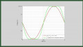
Figure 2, which is also taken from the previous article, illustrates how vF changes if we incorporate different levels of the third-harmonic component.
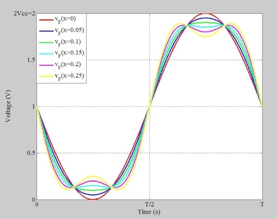
Figure 2. Class F collector voltage for A1 = Vcc = 1 V and values of x varying from 0 to 0.25.
As we increase x from zero to about 0.1, the total voltage becomes flatter around its peaks and troughs. However, as x exceeds 0.1, some ripples appear in the waveform. In this article, we’ll keep things simple by designing for the flattest possible waveforms.
Though we'll bypass the detailed derivation process, the first step of the design procedure is to determine the minimum and maximum limits of the collector voltage waveform (vF from Equation 1). We do this by differentiating vF from Equation 1 and setting the result equal to zero.
Next, we calculate the second derivative of vF and set it to zero at the limits. This establishes a relationship between A1 and A3. The end result is that for a maximally flat waveform, we should have:
$$A_3 ~=~ \frac{1}{9} A_1$$
Equation 2.
By combining Equations 1 and 2, we obtain the maximally flat collector voltage:
$$v_{F} ~=~ V_{cc} ~-~A_1 \big ( \sin(\omega t)~+~ \frac{1}{9} \sin(3 \omega t) \big )$$
Equation 3.
The green curve in Figure 3 plots vF for A1 = Vcc = 1 V and A3 = 0.11, which corresponds to x = 1/9. The sinusoidal red curve (x = 0) is included so that we can more clearly see the flattening of the waveform.
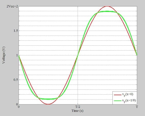
Figure 3. Class F collector voltage for A1 = Vcc = 1 V and x = 1/9.
In the figure above, it’s clear that the available swing (0 to 2Vcc, which in this case is 0 to 2 V) isn’t completely utilized. We can increase the input power at the fundamental component to exploit the full potential swing. To this end, we note that the minimum of vF occurs at ⍵t = π/2. Equating the minimum with 0 V, we obtain:
$$V_{cc}~-~A_1(1~-~\frac{1}{9})~=~0 \quad \rightarrow \quad A_1~=~\frac{9}{8}V_{cc}$$
Equation 4.
Plugging this value of A1 into Equation 3 gives us the maximally flat voltage waveform for full voltage swing:
$$v_{F} ~=~ V_{cc}~-~ \frac{9}{8} \sin(\omega t) ~-~\frac{1}{8} \sin(3 \omega t)$$
Equation 5.
Calculating the Class F Amplifier’s Efficiency
As the preceding article stated more than once—in its closing sentence, even—the Class F amplifier represents an improvement in efficiency over the Class B. Let’s put that to the test in this section.
As always, the amplifier’s theoretical efficiency is equal to the average load power divided by the power drawn from the supply (\(\eta~=~\frac{P_L}{P_{cc}}\)). Using the amplitude of the fundamental voltage component (Equation 4), we can calculate PL as follows:
$$P_L~=~ \frac{v_{o, rms}^2}{R_L}~=~ \frac{1}{2}\frac{ A_1^2}{R_L} \quad \rightarrow \quad P_L ~=~ \frac{81}{128} ~\times~ \frac{V_{cc}^2}{R_L}$$
Equation 6.
which is about 27% greater than for Class B operation.
We calculate the power drawn from the supply by finding the average value of the collector current and multiplying it by the supply voltage (Vcc). With a conduction angle of 180 degrees (π radians), we can assume that the collector current is a half-wave rectified sinusoid of amplitude Ip and period T (Figure 4).
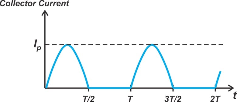
Figure 4. The collector current is a half-wave rectified sinusoid.
Note that while a Class F amplifier’s conduction angle is typically set at 180 degrees in most applications, it can be any value less than 180 degrees.
Using the Fourier series representation, we express the collector current in terms of its constituent frequency components:
$$i_{collector}(t)~=~ \frac{I_p}{\pi} ~+~ \frac{I_p}{2}\sin(\omega_0 t) ~-~ \frac{2I_p}{3\pi} \cos(2 \omega_0t)~-~ \frac{2I_p}{15\pi} \cos(4 \omega_0t) ~+~ …$$
Equation 7.
From Equation 7, the average value of the half-wave rectified signal in Figure 4 is Ip/π. Therefore, the power delivered by the supply is:
$$P_{cc}~=~\frac{I_p V_{cc}}{\pi}$$
Equation 8.
Equations 6 and 8 gave us the amplifier’s load power and supply power, respectively. Before we can use Equation 8 to calculate the efficiency of the amplifier, however, we need to establish a relationship between Ip and Vcc.
The amplitude of the fundamental component is Ip/2. This current flows into the load (RL) and produces a fundamental voltage amplitude of A1 = (9/8)Vcc. Therefore, we obtain:
$$\frac{I_p}{2} ~\times~ R_L ~=~\frac{9}{8} V_{cc} \quad \rightarrow \quad I_p ~=~ \frac{9}{4}\frac{V_{cc}}{R_L}$$
Equation 9.
Combining Equations 8 and 9, we find a new relationship for Pcc:
$$P_{cc}~=~\frac{I_p V_{cc}}{\pi}~=~\frac{9}{4 \pi} ~\times~ \frac{V_{cc}^2}{ R_L}$$
Equation 10.
Finally, using Equations 6 and 10, we can calculate the Class F amplifier’s efficiency:
$$\eta ~=~ \frac{P_L}{P_{cc}} ~=~ \frac{\frac{81}{128} ~\times~ \frac{V_{cc}^2}{R_L}}{\frac{9}{4 \pi} ~\times~ \frac{V_{cc}^2}{ R_L}}~=~\frac{9 \pi}{32}~=~88.4 \ \%$$
Equation 11.
By comparison, the Class B amplifier has a maximum efficiency of:
$$\eta_{max} ~=~ \frac{\pi}{4}~=~78.5 \, \%$$
Equation 12.
The third-harmonic peaking Class F amplifier improves the efficiency by a factor of \(\frac{9}{8}\), or 1.125.
Example: Designing a Third-Harmonic Peaking Class F Amplifier
Let’s wrap up this article with a design example. Determine the following for a third-harmonic peaking Class F amplifier that delivers 50 W to a 50 Ω load:
- The required supply voltage (Vcc).
- The maximum current (Ip) and voltage (2Vcc) that the transistor must tolerate.
- The component values for the fundamental-frequency resonator (L0 and C0 in Figure 1).
Assume that the carrier frequency (fc) is 500 MHz and the required bandwidth (BW) is 75 MHz.
Equation 6 shows the power that a Class F stage with third-harmonic peaking delivers to a load. Substituting PL = 50 W and RL = 50 Ω into this equation, we have:
$$50 ~=~ \frac{81}{128} ~\times~ \frac{V_{cc}^2}{50} ~~\rightarrow~~ V_{cc}~=~ 62.85 \ \text{V}$$
Equation 13.
The required supply voltage is 62.85 V. That makes the maximum voltage across the transistor 125.7 V, since it’s equal to 2Vcc. From Equation 9, the maximum current flowing through the transistor is:
$$I_p ~=~ \frac{9}{4}\frac{V_{cc}}{R_L} ~=~ \frac{9}{4} ~\times~ \frac{62.85}{50}~=~2.83 \ \text{A}$$
Equation 14.
All that’s left now is for us to find the required inductance (L0) and capacitance (C0) of the fundamental-frequency resonator. To do so, we first first need to find the load Q-factor. Using the given carrier frequency (fc = 500 MHz) and bandwidth (BW = 75 MHz) values, we can calculate the Q-factor as follows:
$$Q_L ~=~ \frac{f_c}{BW}~=~\frac{500}{75}~=~6.67$$
Equation 15.
For a parallel-tuned RLC circuit, the Q-factor is related to the component values by the following equation:
$$Q_L ~=~ \frac{R_L}{L \omega_c}~=~{R_L C \omega_c}$$
Equation 16.
Since QL = 6.67 and RL = 50 Ω, the value of L0 works out to:
$$L_0 ~=~ \frac{R_L}{\omega_c Q_L}~=~\frac{50}{2 \pi ~\times~ 500 ~\times~ 10^6 ~\times~ 6.67}~=~2.4 \ \text{nH}$$
Equation 17.
Finally, the required capacitance is:
$$C_0 ~=~ \frac{Q_L}{\omega_c R_L}~=~\frac{6.67}{2 \pi ~\times~ 500 ~\times~ 10^6 ~\times~ 50}~=~42.46 \ \text{pF}$$
Equation 18.
Wrapping Up
A Class B stage has a maximum efficiency of 78.5%. By contrast, a third-harmonic peaking amplifier with maximally flat waveforms exhibits a maximum efficiency of 88.4%. We’ll discuss a more efficient, less-flattened, third-harmonic peaking amplifier in the next article.
This article is Part 22 of a series on power amplifier classes. A complete list of articles in this series is provided below.
Classes A through C:
Class D:
Class E:
Class F and Inverse Class F:
All images used courtesy of Steve Arar