Facebook
 Google
 GitHub
 Linkedin
Introduction to the Class F Power Amplifier
This article explores the basic principles of Class F operation and introduces the third-harmonic-peaking Class F amplifier.
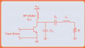
So far, this article series has covered five different power amplifier classes: A, B, C, D, and E. We’re now ready to discuss the sixth, Class F. These amplifiers use a load network with multiple harmonic resonators to boost efficiency and output power. Figure 1 shows the circuit diagram for a basic Class F amplifier.

Figure 1. Circuit diagram for a third-harmonic-peaking Class F amplifier.
This configuration is known as the third-harmonic-peaking Class F amplifier. For comparison purposes, Figure 2 shows the circuit diagram for a single-transistor Class B amplifier.
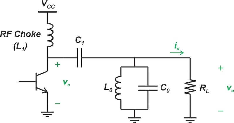
Figure 2. A single-transistor Class B amplifier.
As you can see, the two circuits are quite similar. The only difference is the inclusion of a second resonant circuit. Class F amplifiers shape their voltage waveforms by employing multiple resonant circuits tuned to the signal’s harmonics. The multi-resonant load network keeps the voltage across the transistor low when the current through the transistor is high, producing a square wave.
To understand how this increases efficiency, we first need to take a step back and examine the power dissipation of the Class B stage. Once we’ve done that, we’ll be ready to discuss how Class F operation improves on it.
Power Loss in a Class B Amplifier
Both the Class B and Class F circuit in the previous section include a single transistor. Because achieving high efficiency is of primary importance in power amplifier design, minimizing the transistor’s power dissipation is essential. Power dissipation within the transistor means that the circuit is consuming power from the supply without transferring it to the load. Instead, the power is squandered within the transistor itself, reducing efficiency.
To better understand the Class B transistor’s power dissipation, let’s examine the voltage and current waveforms at its collector. The top plot of Figure 3 shows the collector current waveform for an ideal Class B amplifier. The bottom plot shows the waveform for the collector voltage.
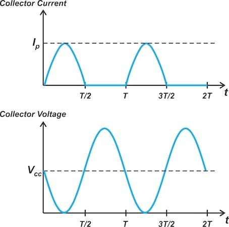
Figure 3. The collector current (top) and collector voltage (bottom) for an ideal Class B stage.
In a Class B amplifier, the transistor is biased just below its turn-ON point and is driven into conduction by the positive half-cycle of the input signal. The collector current is, therefore, a half-wave, rectified sinusoid rich in different harmonics.
As the bottom plot of Figure 3 illustrates, the Class B amplifier’s output voltage is a sinusoid at the fundamental frequency. To faithfully reproduce the input signal, the load network uses a high-Q resonant circuit at the fundamental frequency. The tank shorts the harmonic components, producing the sinusoid we see above.
From Figure 3, it’s evident that the transistor doesn’t dissipate any power during its OFF half-cycle—for example, the interval from t = T/2 to t = T—because zero current flows through the transistor during these time intervals.
During the ON half-cycle (t = 0 to t = T/2), both the transistor current and voltage are non-zero, indicating power loss in the transistor. Luckily, the collector voltage decreases as the current rises. This is beneficial from an efficiency standpoint—an amplifier whose collector voltage maintains a large constant value during the ON half-cycle would exhibit a significantly higher power loss than the Class B stage. In other words, increasing the Class B amplifier’s collector voltage waveform during the ON half-cycle degrades efficiency.
The basic idea of Class F operation is to increase efficiency by doing the opposite—reducing the voltage during the ON-half cycle rather than increasing it. Let’s discuss this further in the next section.
Understanding Class F Operation
Figure 4 shows collector current and voltage waveforms for a Class F amplifier. We can see in the bottom plot that it reduces the voltage waveform below that of the Class B stage during the transistor’s ON half-cycle. Lower voltage when the transistor is ON translates to a smaller current-voltage product, which in turn means that the transistor dissipates less power.
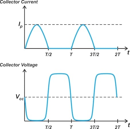
Figure 4. A collector voltage waveform with sharper edges can reduce the power loss in the transistor.
When the collector voltage approaches a rectangular waveform, it reduces the product of the voltage and current. To obtain the lower possible voltages during high-current conditions, we need to make the transitions of the voltage waveform sharper and flatten its peaks and troughs. We can accomplish this by adding harmonic components with appropriate amplitude and phase to the voltage across the transistor.
The Class F circuit in Figure 1, which is known as the third-harmonic-peaking amplifier, represents a common implementation of this idea. As its name suggests, it achieves the desired voltage waveform by adding a third-harmonic component. We’ll examine the circuit itself in the next article of this series. For now, let’s discuss its basic principles with the help of some voltage plots.
Basics of the Third-Harmonic-Peaking Class F Amplifier
Essentially, the third-harmonic-peaking amplifier adds a third-harmonic component to a Class B amplifier. Referring back to Figure 3, we can express the collector voltage for an ideal Class B amplifier as:
$$v_B ~=~ V_{cc} ~-~A_1 \sin(\omega t)$$
Equation 1.
where A1 is the amplitude of the fundamental voltage component. The voltage waveform in Figure 3 corresponds to the maximum output swing (A1 = Vcc).
Next, let’s consider a third-harmonic component of amplitude A3:
$$v_3 = A_3 \sin(3 \omega t)$$
Equation 2.
If we subtract v3 from vB, the new collector voltage works out to:
$$\begin{eqnarray}v_{F} &~=~& V_{cc} ~-~A_1 \sin(\omega t)~-~A_3 \sin(3 \omega t) \\&~=~&V_{cc} ~-~A_1 \Big (\sin(\omega t)~+~x ~\times~ \sin(3 \omega t) \Big )\end{eqnarray}$$
Equation 3.
where x = A3/A1.
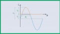
Figure 5 plots vB, v3, and vF for A1 = Vcc = 1 V and A3 = 0.05. In the above equation, x is defined as the ratio of the third-harmonic component (A3) to the fundamental component (A1), so this corresponds to x = 0.05.
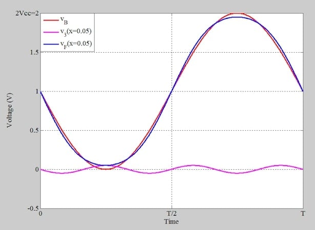
Figure 5. The collector voltage waveform for the Class B amplifier (red), the third-harmonic component (magenta), and the total voltage comprising the fundamental and third harmonic components (blue) for A1 = Vcc = 1 V and x = 0.05.
With the voltage waveforms defined in Equations 1 through 3, the phase difference between the fundamental and third harmonics aligns the fundamental harmonic's trough with the third harmonic's peak. Likewise, the fundamental harmonic's peak is aligned with the third harmonic's trough. As a result, the total or Class F voltage (vF) is slightly flatter around its peaks and troughs compared to the original (vB) waveform, which has no third-harmonic component.
The above waveforms show that with an appropriate phase difference between the two frequency components, we can use a third-harmonic component to flatten the voltage waveform. Note also that while the fundamental component has a peak-to-peak swing of 2A1 = 2Vcc, the composite waveform vF has a smaller peak-to-peak swing of about 0.05 V to 1.95 V. The addition of the third-harmonic component reduces the peak-to-peak swing of the composite waveform.
The collector voltage curve in Figure 5 doesn’t completely utilize the available swing (0 to 2Vcc). To exploit the full potential swing, we increase the input power at the fundamental component. Figure 6 shows the waveforms for Vcc = 1 V, A1 = 1.053 V, and A3 = 0.053 V. These values, like those in the previous example, correspond to x = 0.05.

Figure 6. The collector voltage waveform for the Class B amplifier (red), the third-harmonic component (magenta), and the total voltage consisting of the fundamental and third harmonic components (blue) for Vcc = 1 V, A1 = 1.053, and x = 0.05.
For given swing limits, we can conclude that the addition of the third harmonic allows us to increase the fundamental component (A1). This, in turn, increases the power delivered to the load at the fundamental component.
In the above example, the fundamental component (A1) is increased from 1 V to 1.053 V. As a result, for a given load impedance, the power delivered to the load increases by a factor of 1.0532 = 1.11. In other words, the output power for the third-harmonic-peaking Class F stage increases by about 11% compared to a Class B stage.
What About Increasing the Amplitude of the Third Harmonic?
Figure 7 illustrates how the total voltage waveform (vF) changes for different levels of the third-harmonic component.
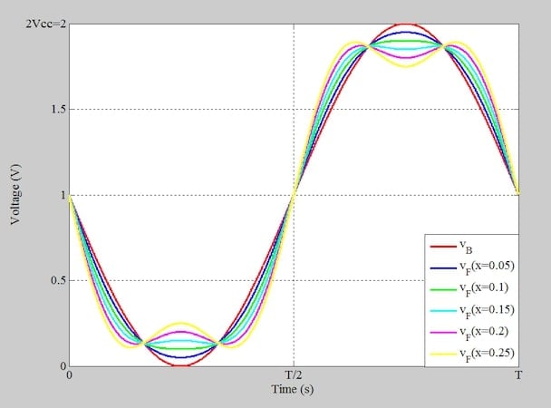
Figure 7. The total collector voltage (vF) for A1 = Vcc = 1 V and x varying from 0.05 to 0.25.
As we increase x from 0.05 to about 0.1, the total voltage becomes flatter around its peaks and troughs. If x exceeds 0.1, however, some ripples appear in the waveform.
Wrapping Up
Based on what we’ve learned so far, the optimal third-harmonic value appears to be the one that shapes the collector voltage into a square wave. In the next article of this series, which continues our discussion of the third-harmonic-peaking Class F amplifier, we’ll see that this isn’t quite true. However, such an amplifier still exhibits far greater efficiency and output power than we would see in a Class B stage.
This article is Part 21 of a series on power amplifier classes. A complete list of articles in this series is provided below.
Classes A through C:
Class D:
Class E:
Class F and Inverse Class F:
All images used courtesy of Steve Arar