Facebook
 Google
 GitHub
 Linkedin
Determining RF Choke Requirements for a Class E Power Amplifier
In this article, we examine the effects of RF choke non-idealities on Class E amplifier performance and learn how to choose the right choke inductance for your amplifier design.
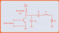
Figure 1 shows the basic topology of a Class E amplifier.

Figure 1. A basic Class E amplifier. The RF choke supplies a DC current of I0.
From previous articles in this series, we know that the RF choke (L1) in the above circuit maintains a nearly constant current of I0. However, those articles all assumed an ideal RF choke with no DC resistance and infinite RF reactance at the frequency of operation. Practical choke inductors have non-zero DC resistance and finite RF reactance.
In this article, we’ll analyze the effects of these imperfections on the performance of Class E power amplifiers. We’ll then put our knowledge into practice by working through two design examples—one related to resistance and one related to inductance. Finally, we’ll test the accuracy of our analysis by simulating our example circuit in LTspice.
The Trade-Off Between Reactance and DC Resistance
The RF choke must have infinite reactance to fully eliminate AC current components and allow only a DC current. This is clearly not possible in practice. Instead, we seek to ensure that the AC current flowing through the choke is much lower than the DC current by increasing the choke inductance.
When doing so, we face an important trade-off between two factors:
- Power loss due to the choke’s DC resistance.
- The ability of the choke to block AC components.
While a larger inductance blocks AC currents more effectively, it also introduces greater DC resistance. As we’ll discuss in the next section, this increases the power dissipation in the choke.
A large inductance also increases the size, weight, and cost of the design. Furthermore, it can introduce a higher parasitic capacitance to the circuit. We therefore aim to use the smallest possible inductance that is still large enough to sufficiently suppress AC components.
We’ll return to the topic of inductance later on. For now, let’s start by determining the power loss caused by the choke’s DC resistance.
Understanding the Effects of Non-Zero Choke Resistance
For an optimally operating Class E amplifier, the DC current flowing through the RF choke (I0) is related to the amplitude of the load current (IR) by the following equation:
$$I_0 ~=~ 0.537 ~\times~ I_R$$
Equation 1.
The flow of I0 through the choke's DC resistance leads to a power loss given by:
$$P_{Loss}~=~ R_{RFC} ~\times~ I_0^2$$
Equation 2.
where RRFC is the DC resistance of the RF choke.
By combining Equations 1 and 2, we obtain the following power loss formula:
$$P_{Loss} ~=~ 0.2884 ~\times~ R_{RFC} I_R^2$$
Equation 3.
Meanwhile, the average power delivered to the load is:
$$P_{L}~=~ \frac{1}{2} R_{L} I_R^2$$
Equation 4.
where RL is the load resistance of the amplifier.
Combining Equations 3 and 4, we can find the ratio of PLoss to PL:
$$\frac{P_{Loss}}{P_L}~=~ 0.5768 ~\times~ \frac{R_{RFC}}{R_L}$$
Equation 5.
We can now apply this equation to determine the efficiency of the Class E amplifier when RRFC isn’t equal to zero.
How Does the Choke’s DC Resistance Affect Efficiency?
To keep things simple, let’s assume the following:
- The choke’s DC resistance (RRFC), though not equal to zero, is small enough not to influence I0 or IR.
- The choke’s DC resistance is the only loss mechanism affecting the amplifier.
Like the switching losses we examined previously, a non-zero RRFC increases the power drawn from the supply (Pcc) but doesn’t significantly affect how much power is delivered to the load (PL). Pcc is equal to the sum of the power delivered to the load (PL) and the power dissipated in the choke (PLoss):
$$P_{cc} ~=~ P_L ~+~ P_{Loss}$$
Equation 6.
The efficiency of the amplifier is then:
$$\eta ~=~ \frac{P_L}{P_{cc}}~=~ \frac{P_L}{P_L + P_{Loss}}~=~\frac{1}{1~+~\frac{P_{Loss}}{P_L}}$$
Equation 7.
Or, if we take Equation 5 into account:
$$\eta ~=~ \frac{1}{1~+~0.5768 ~\times~ \frac{R_{RFC}}{R_L}}$$
Equation 8.
Let’s apply this equation to an example problem.
Example 1: Determining Efficiency When the Choke Has Non-Zero Resistance
Assume that an optimally operating Class E amplifier uses a 400 μH RF choke with a DC resistance of RRFC = 0.3 Ω. What would be the efficiency of the amplifier if the load resistance is RL = 50 Ω? Assume that the non-zero choke resistance is the only loss mechanism affecting the circuit.
Applying Equation 8, we have:
$$\eta ~=~ \frac{1}{1~+~0.5768 ~\times~ \frac{R_{RFC}}{R_L}}~=~ \frac{1}{1~+~0.5768 \times \frac{0.3}{50}}~=~99.7 \ \%$$
Equation 9.
The efficiency of this amplifier is 99.7%. That’s lower than the Class E amplifier’s theoretical efficiency of 100%, but not by much. The more we increase the DC resistance, however, the less efficient the amplifier will become. To avoid increasing RRFC unnecessarily, we want to use the minimum required inductance.
Determining the Required Inductance
In this section, we’ll calculate the peak-to-peak ripple of the current through the RF choke and use it to determine the minimum choke inductance we’ll need for a Class E design. We’ll start by seeing how the choke current changes over the course of one RF cycle.
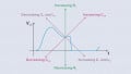
Figure 2 shows three different curves. From top to bottom, these are:
- The current through a Class E amplifier’s switch.
- The voltage across a Class E amplifier’s switch.
- An approximation of the current through an RF choke with finite reactance.
Note that the actual choke current waveform is somewhat different from what’s shown below. Still, this approximate waveform allows us to derive a simple but reasonably accurate equation for the ripple in the RF choke current.

Figure 2. Current through the switch (top), voltage across the switch (middle), and current through the RF choke (bottom).
When the switch turns ON, the collector of the Class E circuit in Figure 1 is grounded (Vsw = 0) and the RF choke sustains a relatively constant voltage of Vcc. The current through an inductor is proportional to the time integral of the voltage across it. Thus, applying a constant voltage to the inductor results in a linear increase in its current.
During the ON state of the switch, we can express the current through the RF choke as:
$$I_{L1}(t) ~=~ \frac{1}{L_1} \int_{0}^{t} V_{cc} \ dt ~+~ i_0 ~=~ \frac{V_{cc}}{L_1} ~\times~ t ~+~ i_0$$
Equation 10.
where i0 is a constant of integration and accounts for the initial current through the inductor at the switch turn-on instant.
With a duty ratio of 50%, the peak value of the current i1 occurs at t = T/2:
$$i_1~=~ \frac{V_{cc}}{L_1} ~\times~ \frac{T}{2} ~+~ i_0$$
Equation 11.
Therefore, the peak-to-peak current ripple is:
$$\Delta I ~=~ i_1 ~-~ i_0 ~=~ \frac{V_{cc}}{L_1} ~\times~ \frac{T}{2}~=~ \frac{V_{cc}}{2fL_1}$$
Equation 12.
For the sake of our analysis, let’s presume that the goal is to keep ΔI below one-tenth of the choke's DC current. Implementing this limitation on Equation 12 yields:
$$\frac{\Delta I}{I_0} ~\leq~ 0.1 ~~\rightarrow~~ L_1 ~\geq~ \frac{5V_{cc}}{f I_0}$$
Equation 13.
To simplify this equation, we need to express I0 in terms of Vcc:
$$I_0 ~=~ 0.577 ~\times~ \frac{V_{cc}}{R_L}$$
Equation 14.
This equation can also be found in “Unraveling the Design Equations of the Class E Power Amplifier.”
Combining Equations 13 and 14, we obtain:
$$L_1 ~\geq~ \frac{8.66 ~\times~ R_{L}}{f }$$
Equation 15.
The above equation allows us to determine the minimum inductance that keeps the peak-to-peak current variation below 10% of the DC current through the choke.
Example 2: Finding the Minimum Choke Inductance
In a previous article, we designed the Class E amplifier shown in Figure 3. It delivers 1.66 W to a 50 Ω load at 1 MHz. Let’s determine the minimum choke inductance required to keep the peak-to-peak variation of the amplifier’s choke current below 10% of its DC value.

Figure 3. Schematic of the Class E amplifier we designed in a previous article.
Note that the component values in this figure were obtained for zero saturation voltage (Vsat = 0) and a load Q-factor of 10.
Applying Equation 15, we have:
$$L_1 ~\geq~ \frac{8.66 ~\times~ R_{L}}{f } ~=~ \frac{8.66 ~\times~ 50}{1 ~\times~ 10^6} ~=~ 433 ~\ \mu \text{H}$$
Equation 16.
According to this analysis, the RF choke must have an inductance of at least 433 μH for the amplifier to achieve optimum performance.
Using LTspice to Review the Class E Amplifier’s Operation
To assess the accuracy of the above analysis, let’s try simulating our example circuit in LTspice. We’ll use the LTspice schematic in Figure 4.

Figure 4. LTspice schematic for simulating the Class E stage in Figure 3.
In the figure above, an ideal switch is used in place of the transistor. The .model statement specifies the following for the switch, which is controlled by voltage source V2:
- An ON-resistance of 0.1 Ω.
- An OFF-resistance of 100 MΩ.
- A threshold voltage of 0.5 V.
Figure 5 shows the simulated switch voltage (Vsw) and choke current (IL1) for this circuit. It also shows the DC supply voltage (Vcc).
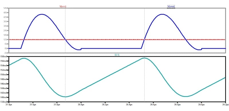
Figure 5. The voltage across the switch (blue), supply voltage (red), and current through the RF choke (turquoise) for the LTspice circuit.
The voltage across the switch is represented by the blue curve in the above figure. It’s almost exactly the switch voltage waveform we would expect from an optimally operating Class E stage, with one difference: it doesn’t fully satisfy the zero-voltage switching condition.
Instead of being at 0 V when the switch turns ON—at just before t = 38 μs, for example—the simulated voltage waveform is slightly negative. It’s a relatively small discrepancy, though you might still consider fine-tuning the circuit components to achieve the best possible performance.
The turquoise curve in Figure 5 shows the current through the RF choke. It’s somewhat different from the choke current waveform shown in Figure 2. There, the current ramps up during the ON state of the switch and discharges during the OFF state—an assumption we carried into the equation we derived for the choke’s minimum inductance.
In the simulated waveforms, the ON state of the switch corresponds to the time interval between t = 38 μs and t = 38.5 μs. However, the simulation shows that the current starts to rise at about t = 37.87 μs, which is some time before the switch turns ON. The current continues its upward trend even after the switch turns OFF, until roughly t = 38.53 μs.
In short, contrary to our assumption that the current ramps up in one half-cycle and discharges in the other, the simulation shows that current rise also occurs in some portions of the switch-OFF half-cycle. But why?
To answer this question, note that Vsw is lower than Vcc from t = 37.87 μs to t = 38.53 μs. This results in a positive voltage across the choke. The current through an inductor is proportional to the time integral of the voltage across it, so it makes sense that the current through the choke increases in this time interval.
The end result is that the peak-to-peak current ripple we found in our analysis is somewhat less than the actual value. In the simulated waveforms, the current changes from 140.33 mA to 157.39 mA and has an average value of I0 = 148.51 mA. The peak-to-peak value is therefore 11.5% of I0, instead of the 10% we expected. Despite that, Equation 15 is still a reasonably accurate way of determining the required choke inductance.
Wrapping Up
Class E power amplifiers are known for their high efficiency. However, a practical Class E amplifier design must take component non-idealities into account. As we saw in this article, the DC resistance of the amplifier’s RF choke causes power dissipation in the choke itself, degrading the efficiency of the amplifier.
Furthermore, the finite reactance of a practical RF choke leads to current ripple that we can’t address without increasing the choke resistance. We therefore want to use the smallest inductance that we can while still suppressing AC components to the necessary degree.
In the next article of this series, we’ll learn how tuning the amplifier can help us achieve optimal performance despite these and other non-idealities. This will be the final article about Class E power amplifiers before we move on to discussing Class F operation.
This article is Part 19 of a series on power amplifier classes. A complete list of articles in this series is provided below.
Classes A through C:
Class D:
Class E:
Class F and Inverse Class F:
All images used courtesy of Steve Arar