Facebook
 Google
 GitHub
 Linkedin
Understanding the Transmission-Line Peaking Class F Amplifier
Learn how this power amplifier uses a quarter-wavelength transmission line to achieve up to 100% efficiency.
So far, our discussion of Class F power amplifiers has revolved around the third-harmonic peaking amplifier. This Class F configuration incorporates a third-harmonic component to make its collector voltage waveform resemble a square wave, enhancing both efficiency and output power. As we learned in the previous article, the maximum efficiency of the third-harmonic peaking amplifier is 90.7%.
We can improve on this efficiency by tuning all higher harmonic components, rather than just the third. In this article, we’ll learn about a Class F amplifier designed to do exactly that. Known as the transmission-line peaking amplifier, it has an efficiency of 100% under ideal conditions and is widely used in VHF (30 to 300 MHz) and UHF (300 MHz to 3 GHz) FM radio transmitters.
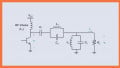
The circuit diagram for the transmission-line peaking amplifier is shown in Figure 1. As you can see, its load network comprises a parallel-resonant circuit and a quarter-wavelength transmission line at the fundamental frequency.

Figure 1. Class F amplifier with a quarter-wavelength transmission line.
To understand how this circuit works, we first need to understand the following:
- The harmonic components required to approximate a square wave.
- The impedance transformation of quarter-wavelength and half-wavelength transmission lines.
We’ll discuss these concepts in the next two sections of the article. After that, we’ll examine the waveforms of an ideal transmission-line peaking amplifier and calculate its efficiency. Finally, we’ll wrap up the article by working through a design example.
Harmonic Contents of a Square Wave
Figure 2 shows a square wave with a peak-to-peak amplitude of A and period T.

Figure 2. A square waveform with peak-to-peak amplitude of A.
The above waveform can be decomposed into its frequency components by employing the Fourier series representation:
$$f(t)~=~\frac{A}{2} ~+~\frac{2A}{\pi} \sin(\omega_{0}t)~+~ \frac{2A}{3\pi}\sin(3\omega_{0}t)~+~\frac{2A}{5\pi}\sin(5\omega_{0}t)~+~...$$
Equation 1.
From Equation 1, we see that a square wave is an infinite series of sinusoids at odd harmonic frequencies. We know that to add a given harmonic component to our waveforms, we need a resonant circuit tuned to that harmonic. Approaching a square wave therefore requires a structure that emulates an infinite array of resonators.
The circuit in Figure 1 achieves this by using a quarter-wavelength line in series with the load. The next section of the article explains how and why this works.
Impedance Transformation of Quarter-Wavelength and Half-Wavelength Lines
The input impedance of a lossless quarter-wavelength line is given by:
$$Z_{in}~=~\frac{Z_0^2}{Z_L}$$
Equation 2.
where:
Z0 is the characteristic impedance of the line
ZL is the load impedance.
We see above that the input impedance of a quarter-wavelength line is inversely proportional to the load impedance. In the case of the transmission-line peaking amplifier, we have a quarter-wavelength transmission line terminated with a short circuit. From Equation 2, the impedance seen at the input of such a line is an open circuit.
Now that we’ve discussed the input impedance, the next step is to examine the load impedance that the collector sees at different harmonic frequencies:
- The fundamental frequency.
- Even harmonic frequencies.
- Odd harmonic frequencies.
We’ll begin with the fundamental frequency.
Load Impedance at the Fundamental Frequency
In Figure 1, the L0-C0 tank is tuned to the fundamental frequency. At this frequency, it acts as an open circuit, causing the quarter-wavelength line to be terminated at RL. Applying Equation 2, the input impedance of the transmission line (as seen by the collector) at the fundamental frequency is a purely resistive value given by:
$$R_{in}~=~\frac{Z_0^2}{R_L}$$
Equation 3.
If the characteristic impedance of the line is equal to the load impedance (Z0 = RL), we obtain Rin = RL.
Load Impedance for Even Harmonics
In Figure 1, the L0-C0 tank shorts the output node to ground at all harmonics. At even harmonics, the length of the line becomes an integer multiple of the half-wavelength of the signal. For example, at the second harmonic, the line is a half-wavelength line. At the fourth harmonic, the line is a full-wavelength line.
When the length of the line is an integer multiple of the half-wavelength, the impedance seen at the input of the line is equal to its load impedance (Zin = ZL). To understand this, we first note that a half-wavelength line can be split into two quarter-wavelength lines.
We can then use Equation 2 to show that the input impedance of a lossless half-wavelength transmission line is equal to its load impedance (ZL), regardless of the characteristic impedance of the line. Therefore, at even harmonics, the collector sees the impedance connected to the right end of the line, which is a short circuit.
Load Impedance for Odd Harmonics
At odd harmonic frequencies, the line effectively becomes an odd multiple of the quarter-wavelength. The short circuit at the output therefore translates into an open circuit at the collector at these frequencies. To understand this, see Equation 1.
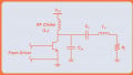
The end result is that the load network is equivalent to an infinite number of parallel-resonant circuits. This is illustrated in Figure 3, which shows the equivalent input impedance at different harmonics for Z0 = RL.

Figure 3. The transmission-line peaking amplifier’s equivalent input impedance at different harmonics for Z0 = RL.
With short-circuit terminations at even harmonics and open-circuit terminations at odd harmonics, the collector voltage waveform is forced to include only the fundamental frequency and odd harmonics. As a result, a square-wave collector voltage is possible.
Waveforms of an Ideal Transmission-Line Peaking Amplifier
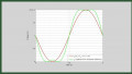
Figure 4 shows the typical waveforms observed in a transmission-line peaking amplifier.

Figure 4. The collector voltage (top), collector current (middle), and load current (bottom) in a transmission-line peaking amplifier.
The signal applied to the input of the transistor is an offset sinusoidal wave that biases the transistor at the device’s turn-ON voltage (corresponding to a conduction angle of 180 degrees). During the ON half-cycle, the collector voltage (vc) is zero.
We know that vc is a square wave. Since there’s no DC voltage drop across an ideal RF choke, we also know that the DC component of vc equals Vcc. With a duty ratio of 50% and vc = 0 during the ON half-cycle, we can conclude that the collector voltage should be equal to 2Vcc during the OFF half-cycle.
A square-wave voltage has all odd harmonic components. However, because the load network presents an open circuit to odd harmonics above the fundamental, it conducts current only at the fundamental frequency. Consequently, the output current (io) is a sinusoidal wave at the fundamental frequency.
This also means that the transistor’s current is sinusoidal during the ON half-cycle. Since the collector current is zero during the OFF half-cycle, the result is a half-sinewave collector current.
To summarize:
- The collector voltage is shaped into a square wave by the high impedances at odd harmonics.
- The collector current is a half-wave rectified sinusoid.
In an ideal scenario, the current and voltage waveforms are identical to those of a Class D amplifier.
Finally, a visual inspection of the above waveforms reveals a phase difference between the fundamental component of vc and io. This is because a current (or voltage) wave experiences a phase difference of 90 degrees when it travels through a quarter-wavelength transmission line. As a result, the fundamental component of vc leads io by 90 degrees.
Calculating the Amplifier's Efficiency
Assume that the collector voltage is a square wave with a peak-to-peak voltage swing of 2Vcc. From the Fourier series representation of the square wave (Equation 1), we know that the amplitude of the fundamental component of vc is:
$$v_{c,1} ~=~ \frac{2}{\pi} ~\times~ 2V_{cc}~=~1.27 ~\times~ V_{cc}$$
Equation 4.
When a transmission line is connected to a matched load, the amplitude of the voltage signal along the length of the transmission line is constant. Therefore, for a matched termination (Z0 = RL), we can conclude that the amplitude of the output voltage is also vo = (4/π)Vcc. Note that the amplitude of vo is larger than Vcc, which is the typical limit of the swing amplitude observed in a Class B amplifier. This is akin to the behavior observed in the third-harmonic peaking amplifier.
The formula for the efficiency of a power amplifier is η = PL/Pcc. If we know the output voltage, we can calculate the average power delivered to the load as follows:
$$P_L~=~ \frac{v_{o, rms}^2}{R_{L}}~=~ \frac{1}{2 R_{L}}(\frac{4}{\pi} V_{cc})^2 \quad \rightarrow \quad P_L ~=~ \frac{8}{ \pi^2} ~\times~ \frac{V_{cc}^2}{R_{L}}$$
Equation 5.
To calculate the supply power, we find the average current drawn from the supply (the average of the middle curve in Figure 3) and multiply it by the supply voltage. We then use the Fourier series representation to express the half-wave rectified collector current as a sum of its frequency components:
$$i_{c}~=~ \frac{I_p}{\pi} ~+~ \frac{I_p}{2} \sin(\omega_0 t) ~-~ \frac{2I_p}{3\pi} \cos(2 \omega_0t)~-~ \frac{2I_p}{15\pi} \cos(4 \omega_0t) ~+~ …$$
Equation 6.
Given that the average collector current is Ip/π, the power output from the supply is calculated as:
$$P_{cc}~=~\frac{I_p V_{cc}}{\pi}$$
Equation 7.
We can use Equations 5 and 7 to calculate the efficiency of the amplifier, but only once we establish a relationship between Ip and Vcc. To do so, we note that the amplitude of the fundamental component of ic is Ip/2. This current flows into the load (RL) and produces a fundamental voltage amplitude of vo = (4/π)Vcc. Therefore, we have:
$$\frac{I_p}{2} ~\times~ R_L~=~\frac{4}{\pi} V_{cc} \quad \rightarrow \quad I_p ~=~\frac{8}{\pi} ~\times~ \frac{V_{cc}}{R_L}$$
Equation 8.
We can now combine Equations 7 and 8 to find the power drawn from the supply:
$$P_{cc}~=~ \frac{8}{\pi^2} ~\times~ \frac{V_{cc}^2}{R_L}$$
Equation 9.
Comparing Equations 5 and 9, we see that the load power and supply power are identical. The theoretical efficiency of the amplifier is therefore 100%.
Note that this is a simplified analysis—we’re assuming that the transistor functions as an ideal switch with zero ON-resistance, infinite OFF-resistance, and no output capacitance. We’re also assuming that the switching action is instantaneous and lossless.
Using the Transmission Line for Impedance Matching
We can design the transmission line to match the external load to the collector impedance. This allows us to maximize the output power at the fundamental frequency.
To calculate the output power for this case, we note that the average power delivered to the input of a lossless line is equal to that delivered to its termination. Applying Equation 4, the output power is then found to be:
$$P_L~=~ \frac{1}{2} ~\times~ \frac{v_{c,1}^2}{R_{in}}~=~ \frac{1}{2 R_{in}}(\frac{4}{\pi} V_{cc})^2 \quad \rightarrow \quad P_L ~=~ \frac{8}{ \pi^2} ~\times~ \frac{V_{cc}^2}{R_{in}}$$
Equation 10.
where Rin is the input impedance of the line.
To help solidify these concepts, let’s work through a design example.
Example: Designing a Transmission-Line Peaking Amplifier
Say that we’re designing a Class F amplifier like the one shown in Figure 1. For this amplifier, the characteristic impedance of the line is Z0 = 50 Ω and the supply voltage is Vcc = 30 V. Determine the following:
- The load impedance (RL) we should use to deliver a power of PL = 7.3 W to the load.
- The maximum current and voltage that the transistor must tolerate.
The first step is to find the required input impedance of the line by applying Equation 10:
$$P_L ~=~ \frac{8}{ \pi^2} ~\times~ \frac{V_{cc}^2}{R_{in}} \quad \rightarrow \quad 7.3 ~=~ \frac{8}{ \pi^2} ~\times~ \frac{30^2}{R_{in}}$$
Equation 11.
Solving for the input impedance gives us Rin ≈ 100 Ω. Now that we have a value for Rin, we use the input impedance equation of the quarter-wavelength line to calculate RL:
$$R_{in}~=~\frac{Z_0^2}{R_L} \quad \rightarrow \quad 100~=~\frac{50^2}{R_L}$$
Equation 12.
which works out to RL = 25 Ω.
From Figure 4, the maximum collector voltage is 2Vcc = 60 V. That just leaves the maximum collector current, which we find by using Rin instead of RL in Equation 8:
$$I_p ~=~\frac{8}{\pi} ~\times~ \frac{V_{cc}}{R_{in}}~=~\frac{8}{\pi} ~\times~ \frac{30}{100}~=~0.76 \ ~ \text{A}$$
Equation 13.
Wrapping Up
A transmission-line peaking Class F amplifier uses a load network consisting of a quarter-wavelength transmission line and a parallel-resonant circuit. The collector voltage comprises the fundamental and odd harmonic components, while the collector current includes the fundamental component along with the even harmonic components. Consequently, power is generated only at the fundamental frequency, resulting in an ideal efficiency of 100%.
As noted earlier, this type of amplifier is widely used in VHF and UHF FM radio transmitters. However, we must keep in mind that implementing the transmission line into a Class F amplifier IC can be challenging due to the required length of the line. Even at a frequency of 2.4 GHz, the quarter-wavelength transmission line is over 3 cm in length.
This article is Part 24 of a series on power amplifier classes. A complete list of articles in this series is provided below.
Classes A through C:
Class D:
Class E:
Class F and Inverse Class F:
All images used courtesy of Steve Arar
Related Content