 Facebook
 Google
 GitHub
 Linkedin
Introduction to Inverse Class F Power Amplifiers
Using the second-harmonic peaking amplifier as an example, we explore the basic principles of inverse Class F amplification.
Class F amplification is a well-established technique that uses harmonic tuning to improve the amplifier’s performance. In a Class F amplifier, odd harmonics are added to the collector voltage to shape it into a square wave. The collector current, which is ideally a half-sine wave, contains the fundamental and even harmonics.
An inverse Class F amplifier, also known as a Class F-1 amplifier, swaps the shape of these waveforms. The collector current is a square wave; the collector voltage is a half-sinusoid. In this article, we’ll examine the simplest member of this family: the inverse Class F amplifier with second-harmonic peaking (Figure 1).

Figure 1. The second-harmonic peaking Class F-1 amplifier.
As you can see, this circuit is identical to the third-harmonic peaking Class F amplifier. The difference is the resonant circuit shown in purple—in the Class F amplifier, it would be tuned to the third harmonic instead of the second.
Inverse Class F Waveforms
The collector waveforms for an ideal inverse Class F amplifier are shown in Figure 2. In practice, we will achieve only an approximation of these waveforms.
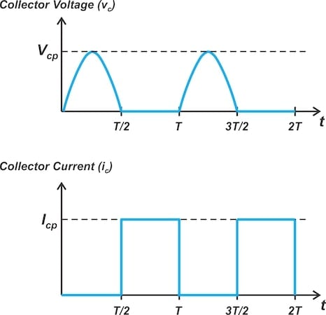
Figure 2. The collector voltage (top) and current (bottom) waveforms in an ideal inverse Class F amplifier.
In the figure above, the voltage across the transistor is zero when the current is high. The same is true of an ideal Class F amplifier (Figure 3).
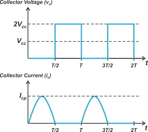
Figure 3. The collector voltage (top) and current (bottom) waveforms in an ideal Class F amplifier.
In both cases, the goal is to improve the amplifier’s efficiency and output power by reducing the current-voltage product as much as possible.
We know that the Class F amplifier produces the square-wave voltage seen at the top of Figure 3 by adding odd harmonic components. To produce a square-wave collector current, an inverse Class F amplifier simply uses a square-wave drive signal at the input of the transistor. But how does it shape the collector voltage into the half-sinusoid we see in Figure 2? Let’s find out.
Shaping the Voltage Waveform
We’ll start by considering some unshaped waveforms. If we remove the L2-C2 harmonic resonator from Figure 1, what’s left is essentially a single-transistor Class B amplifier (Figure 4).

Figure 4. A single-transistor Class B stage.
With no harmonics incorporated, the collector voltage of the Class B stage is an offset sinusoid. This is illustrated, along with the ideal collector current, in Figure 5.

Figure 5. The collector current (top) and voltage (bottom) for an ideal Class B stage.
Our goal is to shape this voltage waveform into a half-sine wave. To make our analysis easier, we’ll set the time origin at the trough of the voltage waveform. This produces the waveforms in Figure 6.

Figure 6. Class B current and voltage waveforms obtained with the adjusted time origin.
In this case, the collector voltage can be expressed as:
$$v_B ~=~ V_{cc} ~-~A_1 \cos(\omega_0 t)$$
Equation 1.
The voltage waveform in Figure 6 corresponds to the maximum swing condition (A1 = Vcc). With that in mind, consider a second-harmonic voltage defined as:
$$v_2 ~=~ A_2 \cos(2 \omega_0 t)$$
Equation 2.
If we add v2 to vB, the new collector voltage works out to:
$$\begin{eqnarray}v_{F} &~=~& V_{cc} ~-~A_1 \cos(\omega_0 t)~+~A_2 \cos(2 \omega_0 t) \\&~=~& V_{cc} ~-~A_1 \Big (\cos(\omega_0 t)~-~x ~\times~ \cos(2 \omega_0 t) \Big )\end{eqnarray}$$
Equation 3.
where x is defined as the ratio of the second-harmonic component to the fundamental component (x = A2/A1).
Figure 7 plots vB, v2, and vF for A1 = Vcc = 1 V and A2 = 0.2 V (x = 0.2).

Figure 7. The collector voltage waveform in a Class B stage (red), a second-harmonic component (magenta), and the composite waveform obtained by adding the second-harmonic component (blue).
Note that the phase difference between the fundamental and second harmonic is chosen so that both the peaks and troughs of vB align with the peaks of the second-harmonic waveform (v2).
Consider the peak point of vB at t = T/2. At this instant, Equation 3 simplifies to Vcc + A1 + A2. Both AC terms are positive, which elevates the peak of the composite (vF) waveform so that it surpasses the peak of the original signal (vB).
At a minimum point such as t = 0, Equation 3 reduces to Vcc – A1 + A2. Due to the AC terms having opposite polarities at this point, their effects negate one another. The result is a leveled composite waveform in the vicinity of t = 0.
This suggests that a second harmonic with appropriate phase can raise the peak of the voltage waveform and flatten its trough. Because the trough of the voltage wave corresponds to the peak of the collector current, this can reduce power loss within the transistor.
The above discussion shows that incorporating a second harmonic produces a composite waveform that roughly approximates a half-sinusoid. Before we move on, note that while the original signal swings from 0 to 2Vcc, the composite waveform swings from 0.2 V to 2Vcc + 0.2 = 2.2 V. We bring the lower voltage swing limit back to ground by setting appropriate values for A1 and A2.
Selecting the Right Amount of Second-Harmonic Component
Figure 8 illustrates how the total voltage waveform (vF) changes if we incorporate different values for the second-harmonic component.

Figure 8. The composite waveform obtained by adding the second-harmonic component for A1 = Vcc = 1 V and x varying from 0 to 0.4.
As x (the ratio of A2 to A1) increases from 0.1 to about 0.3, the total voltage becomes flatter in the vicinity of its trough. When x exceeds 0.3, some ripples appear in the waveform. Based on that, what is the optimal value for the second-harmonic component?
First, we need to define ‘optimal.’ There are two different criteria we could use:
- Producing a maximally flat voltage waveform.
- Producing maximum efficiency.
The first approach keeps the collector voltage as low as possible when the collector current is high. However, it turns out that this waveform doesn’t produce the optimum efficiency—for that, we need a small amount of ripple.
The conditions that yield the maximally flat and maximum efficiency waveforms are outlined below. We’ll bypass the detailed mathematical analysis for now.
The collector voltage is maximally flat when:
$$\frac{A_2}{A_1}~=~\frac{1}{4}$$
Equation 4.
Under this condition and equating the minimum collector voltage to zero, we obtain the absolute values of A1 and A2 in terms of the supply voltage:
$$A_1 ~=~ \frac{4}{3} V_{cc} \quad \text{and} \quad A_2~=~\frac{1}{3} V_{cc}$$
Equation 5.
Meanwhile, the maximum efficiency is achieved for:
$$\frac{A_2}{A_1}~=~\frac{1}{2 \sqrt{2}} ~\approx~ 0.3536$$
Equation 6.
which, keeping the minimum collector voltage at ground, results in the following relationships:
$$A_1 ~=~ \sqrt{2} ~\times~ V_{cc} \quad \text{and} \quad A_2~=~0.5 V_{cc}$$
Equation 7.
Figure 9 plots the collector voltage for the maximally flat and maximum efficiency cases.

Figure 9. The collector voltage waveform obtained for x = 0 (red), maximally flat (blue), and maximum efficiency (green) cases.
Note how the introduction of a second-harmonic voltage into the collector voltage waveform produces an approximate half-sinusoid.
Wrapping Up
Inverse Class F amplifiers seek to minimize power loss by using a square-wave collector current and shaping the collector voltage into a half-sinusoid. In the case of a second-harmonic peaking amplifier, the half-sinusoidal shape is produced—or at least approximated—by incorporating a second-harmonic component. We’ll examine this configuration in more detail and derive its design equations in the next article.
This article is Part 25 of a series on power amplifier classes. A complete list of articles in this series is provided below.
Classes A through C:
Class D:
Class E:
Class F and Inverse Class F:
All images used courtesy of Steve Arar


I never imagined that would be something like inverse class F. It’s very nice, but I didn’t get where you’d use it. Can someone point it?