 Facebook
 Google
 GitHub
 Linkedin
How to Tune a Class E Amplifier
In this article, we discuss a tuning method designed specifically for Class E RF amplifiers.
In previous articles, we delved into the theoretical workings of Class E amplifiers. We also discussed several non-idealities—the non-zero switching times of practical transistors, for example—that cause deviations from this theoretical ideal. Practical Class E amplifiers must also account for the tolerance of electronic components and the presence of parasitic elements in the circuit. Otherwise, these effects will lead to a mistuned amplifier and an accompanying drop in performance.
While we can’t fully eliminate component non-idealities, it is possible to correct for them. In this article, we’ll explore a well-established tuning method designed specifically for Class E amplifiers. Even without knowing the precise values of the load network components, we can use this procedure to fine-tune component values for optimal performance.
Tuning for Optimal Amplifier Performance
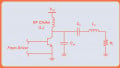
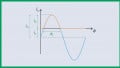
Figure 1 shows the basic topology of a Class E stage.

Figure 1. Schematic of a basic Class E amplifier. Image used courtesy of Steve Arar
To determine the component values for this circuit, we use the design equations presented earlier in this article series. Though Class E amplifiers are somewhat resilient to changes in circuit parameters, we should still plan on tuning the component values to obtain optimum performance. Figure 2 contrasts the typical switch waveforms for properly tuned and mistuned amplifiers.

Figure 2. Typical switch waveforms for optimally operating and mistuned Class E amplifiers. The improperly-tuned case is denoted by “general.” Image used courtesy of F. Raab
The optimum waveforms have the following characteristics:
- When the switch turns ON, the voltage across it is zero.
- The slope of the switch voltage is zero at the instant the switch turns ON.
- The switch duty ratio is 50%.
When these conditions aren’t met, we obtain optimum operation by re-tuning the amplifier. In the coming sections, we’ll discuss how we do (and don’t) accomplish this.
Finding a Reliable Tuning Indicator
We can’t use the DC input power (Pin) or the RF output power (Pout) as indicators for tuning a Class E amplifier. To understand why not, we first need to consider the impedance phase angle (ѱ) of the amplifier’s load network. We can also refer to this as the load angle.
For an optimum Class E amplifier, the effective impedance of the series RLC circuit at the fundamental frequency is given by:
$$Z_L ~=~ R_L ~\times~ (1~+~j1.1525)$$
Equation 1.
We observe from this that the optimum load angle is ѱ = tan-1(1.1525) = 49.052 degrees.
Next, let’s examine how Pin, Pout, and the efficiency (η) vary with the load angle. These relationships are plotted in Figure 3. Note that the input power and output power are denoted by Pi and Po in this figure.
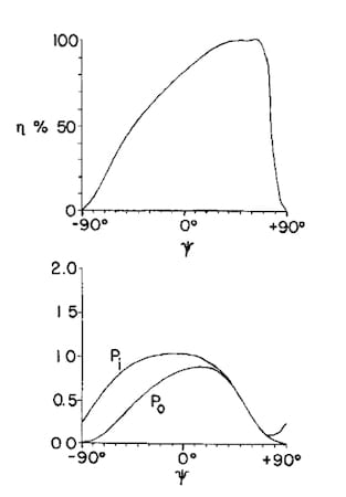
Figure 3. Top plot: Efficiency as a function of the load angle. Bottom plot: Input power and output power as functions of the load angle. Image used courtesy of F. Raab
This plot shows that the maximum of η, Pin, and Pout occur at different load angle values:
- The efficiency (η) reaches its maximum at ѱ = 49 degrees and 65 degrees.
- The DC input power (Pin) reaches its maximum at ѱ = –5 degrees.
- The RF output power (Pout) reaches its maximum at ѱ = 10 degrees.
Of these three parameters, only the efficiency has a maximum value close to the optimum load angle (ѱ = 49.052 degrees). From this, it’s apparent that we can’t use Pin or Pout as tuning indicators.
We could determine the collector efficiency by measuring both Pin and Pout, then use this information to tune the amplifier. However, this method is both tedious and relatively impractical.
Instead, we’ll discuss an established tuning method for Class E amplifiers that hinges on analyzing the switch voltage waveform. This approach allows us to build an optimal Class E amplifier without knowing the exact value of the component values or the parasitic elements within the load network.
Variations in Circuit Parameters Change the Switch Voltage Waveform
For an improperly tuned amplifier, the voltage across the switch has a peak and a trough, as depicted in Figure 4.

Figure 4. Typical switch voltage waveform for an improperly tuned amplifier. Image used courtesy of N. O. Sokal
The location of the trough changes in a predictable way if we change the values of the following circuit components:
- The shunt capacitor (Csh).
- The capacitor of the RLC circuit (C0).
- The inductor of the RLC circuit (L0).
- The load resistor (RL).
This is illustrated in Figure 5.
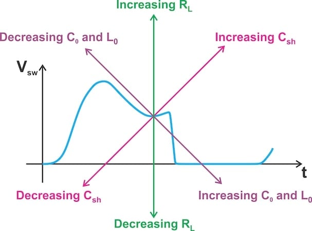
Figure 5. The location of the trough changes as we change Csh, L0, and C0. Image used courtesy of Steve Arar
To summarize the above figure:
- Increasing Csh moves the trough of the waveform upwards and to the right.
- Increasing C0 and L0 moves the trough downwards and to the right.
- Increasing RL moves the trough upwards.
Note that RL isn’t normally an adjustable parameter of RF circuits. It’s included above for the sake of completeness. Instead, we tune the amplifier by adjusting the values of L0, C0, and Csh.
The Tuning Procedure
Now that we know which parameters to adjust, we’re ready to walk through the tuning process. Let’s go through it step by step.
Step 1: Determine the Series Inductance
For a given load resistance (RL) and Q-factor, we choose the appropriate inductance (L0) using the following relationship:
$$L_{0} ~=~ \frac{Q R_L}{\omega}$$
Equation 2.
where ω is the angular frequency. We'll assume that RL, L0, and the frequency of operation retain their nominal values throughout the tuning process.
Step 2: Adjust the Supply Voltage and Duty Cycle
After completing Step 1, we apply a low DC supply voltage (around 4 V) to the circuit and adjust the duty ratio to 50%. The idea of using a low supply voltage is to prevent damage to the transistor while tuning the amplifier. A mistuned amplifier may generate excessive collector voltage or power dissipation.
To determine the duty ratio, we need to know exactly when the transistor switches. However, the switching instants may not be clear from the collector voltage waveform. When that’s the case, N. O. Sokal suggests examining the base voltage (VBE) waveform instead. He identifies the turn-ON point as the moment the rising edge of VBE reaches +0.8 V and the turn-OFF point as the moment when the falling edge of VBE drops to 0 V.
Step 3: Find the Trough and Adjust the Capacitances
Next, we find the trough of the voltage waveform. Based on the position of the trough, we then adjust Csh and C0. For example, consider the mistuned switch voltage waveform in Figure 6. The vertical arrow in this figure points to the transistor turn-ON instant.

Figure 6. Switch voltage turn-ON in a mistuned amplifier. Image used courtesy of N. O. Sokal
To match the optimum waveforms, the trough of this waveform must move downwards and to the left. Referring back to Figure 5, we observe that we need to decrease Csh for this to occur.
In the above example, note that the trough of the waveform is actually hidden from view due to the chosen component values. The switch actually turns ON before the voltage across the shunt capacitor can reach the trough. In cases when the trough isn’t observable, we can estimate its location by visually inspecting the waveform.
Step 4: Return the Supply Voltage to the Nominal Level
Next, we progressively increase the DC supply voltage (Vcc) until it reaches its nominal level. In the paper I linked to above, N. O. Sokal recommends increasing Vcc by up to 50% each time. Because the transistor’s collector-base capacitance diminishes with higher supply voltages, we may need to readjust Csh, C0, and the duty ratio after each incremental increase of Vcc. This need arises because the collector-base capacitance modifies the effective value of Csh.
Step 5: Verify the Results of Tuning
When the tuning procedure is done correctly, we should obtain an optimum voltage waveform similar to what we see in Figure 7.

Figure 7. Switch voltage waveform in a properly tuned amplifier. Image used courtesy of N. O. Sokal
The final step is to perform a tuning verification by slightly increasing Csh. This adjustment should result in a distinct downward step in the voltage waveform at the turn-ON instant, similar to what we observed in Figure 6. This indicates the precise moment the switch turns ON, allowing us to easily verify that the duty ratio is 50% and the slope of the voltage waveform is zero at the turn-on instant.
Once these characteristics are confirmed, we can readjust Csh to its original value, which brings us back to the optimum waveform.
Wrapping Up
In this article, we discussed a Class-E-specific tuning method that allows us to obtain optimal performance even with non-ideal load network components. We can summarize this procedure as follows:
- Choose the appropriate series inductance for the load resistance, Q-factor, and frequency of operation.
- Apply a low DC supply voltage to the circuit and adjust the duty ratio to 50%.
- Find the trough of the resulting switch voltage waveform, then adjust the capacitances (Csh and C0) until the trough is in the desired place. Refer to Figure 5 to see how each component value affects the waveform.
- Increase the DC supply voltage to its nominal level by 50% increments, readjusting the capacitances and the duty ratio as needed.
- Verify the results by slightly increasing the shunt capacitance and observing how it affects the voltage waveform when the switch turns ON.
This is the last article in this series focused on Class E power amplifiers. The next article will introduce the Class F power amplifier. Stay tuned (so to speak)!
References
- “Class-E RF Power Amplifiers” by N. O. Sokal.
- “RF Power Amplifiers” by M. Albulet.
- “Effects of Circuit Variations on the Class E Tuned Power Amplifier” by F. Raab.
This article is Part 20 of a series on power amplifier classes. A complete list of articles in this series is provided below.
Classes A through C:
Class D:
Class E:
Class F and Inverse Class F:


“Who can explain to me why there is equation 1?”