Facebook
 Google
 GitHub
 Linkedin
Protocol, Link, & Physical: Synopsys Debuts First ‘Complete’ Storage
The flash storage solution is the first complete IP set to include UFS 5.0, UniPro 3.0, and M PHY v6.0—and it delivers double the speed of UFS 4.0.
Synopsys broke onto the AI flash storage scene with a recent IP announcement. Synopsys is enabling a new generation of high-speed, low-power, high-efficiency storage for mobile edge-AI devices with this new IP set. The IP stack covers UFS 5.0, UniPro 3.0, and M‑PHY v6.0 storage and communications specifications. Synopsys has verified the performance with successful tape-out on TSMC’s N2/N2P process nodes.
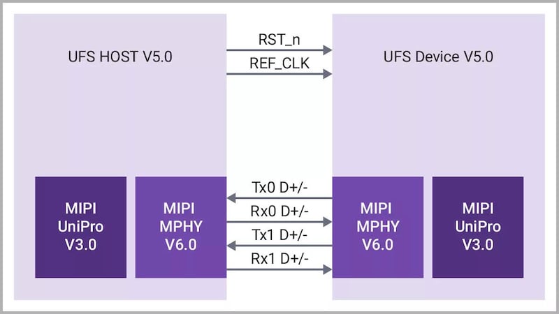
Synopsys UFS 5.0 protocol stack through PHY.
Flash memory capability has not kept up with other parts of edge-AI computing systems. As such, it has become a system-level constraint. The new protocols address this inequality by upping the data rates and improving error correction.
JEDEC manages the UFS standard, and Mobile Industry Processor Interface (MIPI) manages M-PHY and UniPro. The two associations collaborated on this new set of protocols to deliver higher speeds, improved signal integrity, and simplified power-supply integration. The result is a flash specification delivering sequential read and write speeds of up to 10.8 GB/s—double the UFS 4.0 transfer speed limit.
M‑PHY v6.0
MIPI M-PHY is the physical layer covering flash memory storage and chip-to-chip inter-processor communication (IPC) applications. V6.0 of the specification doubles the data rate from V5.0 through the use of pulse amplitude modulation 4 (PAM-4) signaling.
PAM-4 provides four distinct amplitudes in the same time domain as a conventional digital signal would give two. Traditional non-return-to-zero (NRZ) encoding assigns a 0 or 1 to each signal.
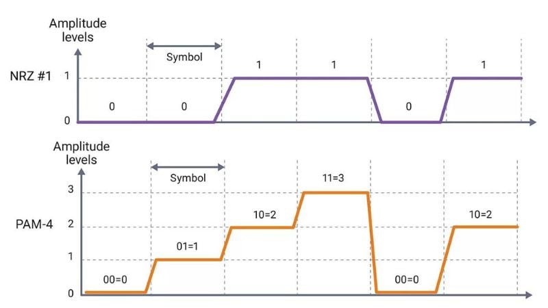
NRZ encoding (possible values per signal are 0 or 1) and PAM-4 encoding (possible values per signal: 00, 01, 10, 11).
PAM-4 encoding has been included in high-speed Ethernet and other leading-edge protocols for some time now. It is new to mobile flash storage with M-PHY 6.0. Doubling the data rate for the same frequency enables a transfer increase without additional hardware lanes. However, it does increase noise sensitivity. The 6.0 specification includes forward error correction and transmitter equalization to address the increased noise sensitivity at higher speeds.
M-PHY 6.0 also moves from 8b10b or 128b130b encoding to 1b1b. 1b1b means that every bit in the stream is a data or command bit. 8b10b uses eight bits out of a 10-bit packet for data/command and two bits for high-/low-load balancing. 128b130b uses a 130-bit packet with two bits for balancing. 1b1b utilizes better circuitry to eliminate the overhead (unusable) bits from the earlier encoding schemes.
UniPro 3.0
MIPI UniPro 3.0 is an application-agnostic transport layer for chip-to-chip/interprocessor communication (IPC) applications. It starts with the abstraction layer that sits on top of M-PHY. From there, it rounds out the device management entity (DME) section by covering the data link, network, and transport layers.
UniPro 3.0 supports up to 46.6 Gbps per lane per direction. Its transport framing structure (TFS) comes from 64-bit cyclic redundancy check (CRC), TFS data scrambling, gray coding, precoding and lane alignment features, and Reed-Solomon forward error correction (RS-FEC). Finally, 3.0 mandates high-speed link start-up (using M-PHY HS-G1 Rate A) to reduce start-up latency.
UFS 5.0
Universal Flash Storage (UFS) 5.0 puts it all together as the next-generation flash storage standard designed for AI, mobile, and automotive devices. UFS 5.0 capitalizes on the improvements from UniPro 3.0 and M-PHY 6.0 to deliver Flash that is twice as fast as UFS 4.0 for edge AI system-on-chip (SoC) storage and local storage in mobile and automotive devices. Synopsys IP supports all UFS 5.0 specification requirements.
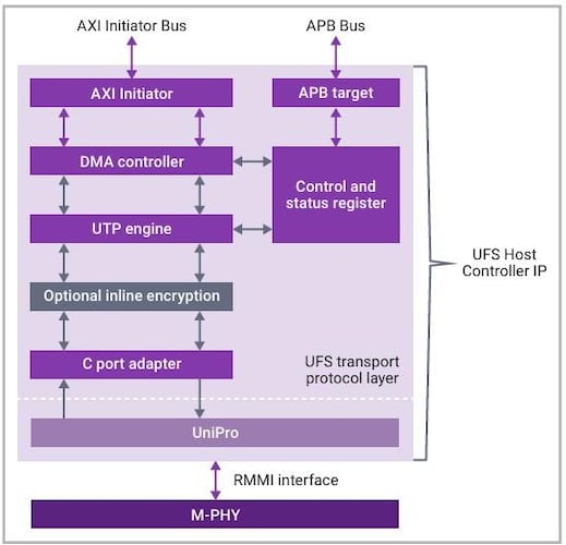
Synopsys UFS 5.0 host controller IP block diagram.
The host controller IP supports a 256-bit SoC system bus and DMA to reduce the processor resources required to support flash. Security is also an important part of edge AI and mobile computing. The Synopsys IP covers this with UFSHCI AES-XTS encryption/decryption in block form, supporting 128- and 256-bit keys.
First With Silicon on TSMC’s N2P
TSMC’s 2-nm process nodes, N2 and N2P (N2 first taped out in 2025 and N2P in 2026), are based on gate-all-around (GAA) nanosheet transistors that reduce leakage and improve power efficiency compared to prior FinFET transistors. N2P improves speeds by 18%, reduces power consumption by 36%, and reduces chip density by 15% over their prior N3E node. Synopsys IP on N2 and N2P delivers a faster protocol stack atop more efficient silicon.
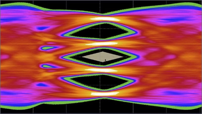
Eye diagram of Synopsys M-PHY v6.0.
Synopsys packages up the flash IP set with databooks, application notes, Verilog RTL source code, Synopsys's design compiler synthesis scripts, and verification configurations.
All images used courtesy of Synopsys.