 Facebook
 Google
 GitHub
 Linkedin
How to Build a Class-D Power Amp
Learn how to build your own Class D power amplifier—one of the most efficient ways to listen to music.
The mighty Class-D amplifier—build one yourself and be amazed by its efficiency. The heat sink barely gets warm!
Have you always wanted to build your own audio power amplifier? An electronic project where you not only see the results but also hear them?
If your answer is yes, then you should continue reading this article on how to build your own Class D amplifier. I will explain to you how they work and then guide you step by step to make the magic happen all by yourself.
Theoretical Basics
What is a Class-D audio power amplifier? The answer could be just a sentence long: It is a switching amplifier. But in order to fully understand how one works, I need to teach you all its nooks and crannies.
Let's start with that first sentence. Traditional amplifiers, like the class AB, operate as linear devices. Compare this to switching amplifiers, so called because the power transistors (the MOSFETs) are acting like switches, changing their state from OFF to ON. This allows a very high efficiency, up to 80 - 95%. Because of this, the amplifier does not generate a lot of heat and does not require a big heat sink like linear class AB amplifiers do. For comparison, the class B amplifier can only achieve a maximum efficiency of 78.5% (in theory).
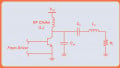
Below you can see the block diagram of a basic PWM Class-D amplifier, just like the one that we are building.

The input signal is converted into a pulse width modulated, rectangular signal using a comparator. This basically means that the input is encoded into the duty cycle of the rectangular pulses. The rectangular signal is amplified, and then a low-pass filter results in a higher-power version of the original analog signal.
There are other methods for converting the signal into pulses, such as ΔΣ (delta-sigma) modulation, but for this project we will be using PWM.
Pulse-Width Modulation Using a Comparator
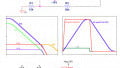
In the plot below, you can see how we transform a sinusoidal signal (the input) into a rectangular signal by comparing it to a triangle signal.

Click to enlarge
At the positive peak of the sine wave, the duty cycle of the rectangular pulse is 100% whilst at the negative peak it is 0%. The actual frequency of the triangle signal is much higher, on the order of hundreds of kHz, so that we can later extract our original signal.
A real filter, not an ideal one, does not have a perfect "brick-wall" transition from passband to stopband, so we want the triangle signal to have a frequency at least 10 times higher than 20KHz, which is the upper human hearing limit.
Power Stage—It All Sounds Good in Theory
Theory is one aspect and practice is another. If we want to put the previous block diagram into practice, we will stumble upon some problems.
Two issues are the rise and fall time of the devices in the power stage and the fact that we are using an NMOS transistor for the high-side driver.

Because the switching of the MOSFETs is not done instantaneously, but is more like going up and down a hill, the transistors' ON time will overlap, creating a low-impedance connection between the positive and negative power supply rails. This causes a high current pulse to pass through our MOSFETs, which can lead to failure.
To prevent this, we need to insert some dead-time between the signals that drive the high and low side MOSFETs. One way to achieve this is to use a specialized MOSFET driver from International Rectifier (Infineon), such as the IR2110S or IR2011S. Furthermore, these ICs provide the boosted gate voltage needed for the high-side NMOS.

Low-Pass Filter
For the filtering stage, one of the best ways to do this is to use a Butterworth filter.

These types of filters have a very flat response in the passband. This means that the signal that we want to achieve will not be attenuated too much.
We want to filter frequencies that are higher than 20 kHz. The cut-off frequency is calculated at -3dB, so we want it to be a bit higher in order to not filter sounds that we want to hear. It is best to choose something between 40 and 60 kHz. The quality factor \[Q = \frac{1}{\sqrt{2}}\].
These are the formulas used to calculate the values of the inductor and the capacitor:
\[L = \frac{R_{L}\sqrt{2}}{2\cdot \pi \cdot f_{c}}\]
\[C = \frac{1}{2\sqrt{2}\cdot \pi \cdot f_{c}\cdot R_{L}}\]
Building Your DIY Amplifier (Luke-The-Warm)
Now that we know how a Class-D amplifier works, let's build one.
First of all, I named this amplifier Luke-The-Warm because the heat sink only barely gets warm, as opposed to a Class AB amplifier, whose heat sink can get quite hot if not actively cooled.
Below you can see the schematic of the amplifier that I designed. It is based on the IRAUDAMP1 reference design by International Rectifier (Infineon). The main difference is that instead of ΔΣ modulation, mine uses PWM.

Click to enlarge
I will now tell you some design choices and how the components work with each other. Let's start from the left side.
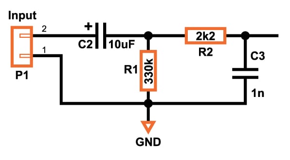
Input Circuitry
For the input circuitry, I decided that it was best to use a high-pass filter followed by a low-pass filter. It is that simple.
Triangle Generator
For the triangle generator, I used an LMC555, which is the CMOS variant of the famous 555 chip. The charging and discharging of the capacitor produces a nice triangle, which is not perfect (it rises and falls exponentially) but if the rise and fall times are equal, it works perfectly.
The values of the resistor and the capacitor set a frequency of approximately 200kHz. Any higher than this and we will run into trouble because the comparator and the MOSFET driver are not the fastest devices.

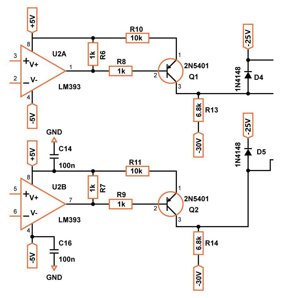
Comparator
For the comparator, you can use whichever component you want—it just needs to be fast. I used what I had available, the LM393AP. At 300ns response time, it is not the fastest and can definitely be improved but it does the job. If you want to use other ICs, just be careful to check that the pins match or you will have to modify the PCB design.
In theory, an op-amp can be used as a comparator, but in reality op-amps are designed for other types of work, so make sure you use an actual comparator.
Because we need two outputs from the comparator, one for the high-side driver and one for the low-side driver, I decided to use the LM393AP. This is two comparators in one package, and we just swap the inputs for the second comparator. Another approach is to use a comparator that has two outputs, such as the LT1016 from Linear Technology. These devices may offer somewhat improved performance, but they could also be more expensive.
These comparators are powered by a 5V bipolar supply, provided by two zener diodes that regulate voltage from the main power supply, which is ±30V.
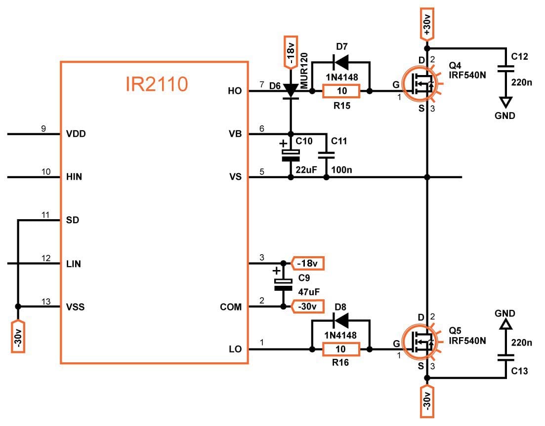
MOSFET Driver
For the MOSFET driver, I chose to use the IR2110. An alternative is the IR2011, which is used in the reference design. This integrated circuit makes sure to add that dead time that I talked about in the previous section.
Because the VSS pin of the IC is tied to the negative power supply, we need to level shift the signals from the comparator. This is done using PNP transistor and 1N4148 diodes.
To drive the MOSFETs, we power the IR2110 with 12V referenced to the negative power supply voltage; this voltage is generated using a BD241 in conjunction with a 12V zener. The high side MOSFET needs to be driven by a gate voltage that is about 12V above the switching node, VS. This requires a voltage that is higher than the positive supply; the IR2110 provides this drive voltage with the help of our bootstrap capacitor, C10.
Filter
Finally the filter. The cut-off frequency is 40kHz, and the load resistance is 4 ohms because we have a 4-ohm speaker (the values used here will also work with an 8-ohm speaker, but it is best to adjust the filter according to the speaker you choose). With this information we can calculate the values of the inductor and the capacitor:
\[L = \frac{4\sqrt{2}}{2\cdot \pi \cdot 40000} H = 22.508\mu H\]
We can safely round down to 22µH.
\[C = \frac{1}{2\sqrt{2}\cdot \pi \cdot 40000\cdot 4} F = 0.703\mu H\]
The closest standard value is 680nF.
Notes on Build
Now that you know all about the inner workings, all you have to do is read very carefully the next few lines, download the files below, buy the components needed, etch the PCB, and start assembling.
Low-Pass Filter
For the low-pass filter, you can use a 680nF capacitor to get as close as possible to the calculated value, but you can also use a 1µF capacitor without any trouble (I designed the PCB so that you can use two capacitors in parallel to mix and match).
These capacitors need to be polypropylene or polyester—in general it's not a great idea to use ceramic capacitors with audio signals. And you need to make sure that the capacitors that you are using for filtering are rated for high voltage, at least 100VAC (more doesn't hurt). The rest of the capacitors in the design also need to have an appropiate voltage rating.
I designed this amplifier for an output power of about 100-150W. You should use a bipolar power supply with ±30V rails. You can go higher than this, but for voltages of about ±40V you need to make sure that you change the values of the resistors R4 and R5 to 2K2.
It is not necessary but highly recommended that you use a heatsink for BD241C as it gets quite hot.
MOSFETs
As far as power MOSFETs go, I suggest using the IRF540N or the IRFB41N15D. These MOSFETs have low gate charge for faster switching and low RDS(on) for lower power consumption. You also need to ensure that the MOSFET has an adequate maximum VDS (drain-to-source voltage) rating. You could use the IRF640N, but the RDS(on) is significantly higher, leading to an amplifier with lower efficiency. Here is a table comparing these three MOSFETs:
| MOSFET | Max VDS (V) | ID (A) | Qg (nC) | RDS(on) (Ω) |
|---|---|---|---|---|
| IRFB41N15D | 150 | 41 | 72 | 0.045 |
| IRF540N | 100 | 33 | 71 | 0.044 |
| IRF640N | 200 | 18 | 67 | 0.15 |
Inductor
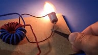
Now the inductor. You can buy one already made but I would suggest that you wind your own—this is a DIY project after all.
Buy a T106-2 toroid. It needs to be iron powder; ferrite can work but it will need a gap or it will saturate. Using the said toroid, wind 40 turns of 0.8-1mm diameter (AWG20-18) copper enameled wire. That's it. Don't worry if it isn't perfect—just make it tight.
Resistors
Finally, all the resistors, unless noted (R4, R5), are 1/4W.
Testing
When I designed the PCB, I made it so that it is very easy to test. The input signal has its own connector and there are two spade terminals for ground: one for the power supply and one for the speaker.
To remove the hum noise (50/60 Hz, from the mains frequency), I used a star-ground configuration; this means connecting all grounds (amplifier ground, signal ground, and speaker ground) at the same point, preferably on the power supply PCB, after the rectifier circuit.
The complete Bill of Materials can be found in the files below, where you can also find the PCB files both in PDF format and as KiCAD files.
Final Thoughts
I hope that the information in this article is sufficient for you to build your own audio power amplifier. I hope it also gets you excited about building your own amplifier.

There are many things that can be improved in this project. You have all the necessary information and files, but you do not need to follow them to the letter.
You can use SMD components, improve the comparator circuit by using a complementary output one, or try the IR2011S instead of the IR2110. Just fire up that soldering iron, etch your PCB, and start working. It does not matter if it does not work on the first try.
It's all about trial and error. When you will finally hear that crisp sound coming from your speaker, it will all be worth it.
If you have any trouble with your build, comment here or post on the forum using as much information as possible. We will work it out.
Give this project a try for yourself! Get the BOM.


An interesting article, and well done to help understand these amps.
A couple of points though..
I feel the “+12V” and “+5V2” would be better labeled as “-18V” and “-25V”.
As you have them it is rather confusing, even though you mention they are referenced to the -30V line.