Facebook
 Google
 GitHub
 Linkedin
How to Increase Slew Rate in Op Amps
Learn how to get faster composite op-amp dynamics by raising the slew rate.
This article is the fourth in a series on amplifiers. In the first article, we discussed how to boost an op-amp’s output current drive capability. In the second, we discussed how to learn more about the method from Part 1 by simulating our voltage buffer circuit in PSpice. In the previous piece, Part 3 of the series, we learned about one method of achieving faster op-amp dynamics: expanding the frequency bandwidth.
Now, we will learn about another method for achieving faster op-amp dynamics: raising our op-amp's slew rate.
Raising the Slew-Rate
The fast dynamics (wide bandwidth as well as high slew rate) and low-distortion characteristics of current-feedback amplifiers (CFAs) make them suited to high-speed applications.
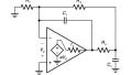
Voltage-feedback amplifiers (VFAs), on the other hand, offer better DC characteristics (low input offset voltage and bias currents, low thermal drift), low noise, and high loop gain, so they are better suited to precision applications. Figure 1(a) shows a composite amplifier that combines the best of both.
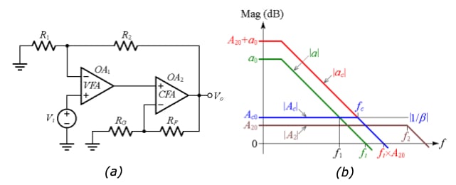
Figure 1. (a) Composite amplifier to achieve a higher slew rate using a current-feedback amplifier (CFA). (b) Straight-line Bode plots,
Figure 1(b), meanwhile, shows straight-line Bode plots where:
- |a| is the open-loop gain of the VFA, and ft is its transition frequency (ft = GBP in the present rendition)
- |ac| is the composite amplifier’s open-loop gain
- |A2| is the closed-loop gain of the CFA, and f2 is its –3-dB frequency
- |Ac| is the composite amplifier’s closed-loop gain, and fc is its –3-dB frequency
- |β| is the feedback factor around the composite amplifier
- a0, Ac0, and A20 identify the DC values of the above gains
The circuit is similar to that of Figure 1(a) from the previous article, shown below.
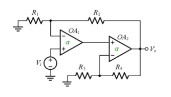
However, the spirit of our new circuit is quite different.
OA2 is no longer an op-amp of the same type as OA1, but rather a much faster device, whose pole frequency f2 is designed to be way above OA1’s ft, so it won’t erode the phase margin of the composite amplifier. As shown in Figure 1(b), the presence of OA2 up-shifts the entire open-loop gain |a| of OA1, to create the composite open-loop gain |ac|.
Given the value of |1/β| as dictated by the application at hand, how do we specify the value of A20 relative to |1/β|? The answer is to impose
\[A_{20} \leq \left | \frac {1}{\beta} \right |\]
(Certainly, we cannot make A20 > |1/β| because this would position the crossover frequency fc above ft, where higher frequency poles of |ac| would destabilize the circuit.)
To gain better insight, consider the PSpice circuit of Figure 2, simulating a 741 op-amp and using a Laplace block to simulate a CFA configured for A20 = 10 V/V (= 20 dB) and f2 = 50 MHz. In this example, we have applied the above equation with the “=” sign.
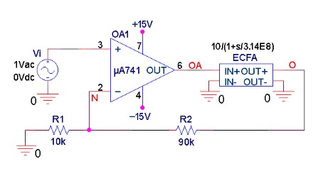
Figure 2. A composite amplifier to raise the SR of the 741 op-amp.
With reference to Figure 3(a), we find it instructive that OA1 has to amplify only by 0 dB, whereas the amplification by 10 V/V is done by the CFA. Smaller output voltage swings by OA1 ought to ameliorate the slew-rate (SR) considerably.
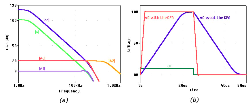
Figure 3. Plots for the PSpice circuit of Figure 2 showing the situation in (a) the frequency domain and in (b) the time domain.
Sure enough, the time response of Figure 3(b), obtained by changing the input source of Figure 2 to a pulse type, confirms our expectation. In the absence of the CFA, the 741 would take about 20 μs to swing by 10 V, so SR = 10/20 = 0.5 V/μs, in accordance with the datasheet. With the CFA in place, the SR of the composite amplifier is an order of magnitude faster, or about 5 V/μs.
We also note an order-of-magnitude increase both in the DC loop gain and in the –3-dB frequency bandwidth of the composite amplifier.
Let's recall Equation 1 from the previous article:
\[f_B = \frac {GBP}{A}\]
According to this equation, a gain of 10 V/V would imply a –3-dB frequency of 100 kHz, whereas the actual measured value is 1.4 MHz. This, thanks to the helping hand provided by the CFA.
Finally, we point out that any overheating by the output stage of the CFA will never reach the input stage of the VFA, thus reducing significantly the effects of input thermal drift.
Also, CFAs typically offer much higher output current drive capabilities than VFAs, so the CFA can be used to raise not only the SR, but also the output current drive capability of the VFA, thus avoiding the need for an output buffer.
In the next article, we will see how to achieve higher DC precision and lower phase distortion.