 Facebook
 Google
 GitHub
 Linkedin
Voltage Buffer Simulation in PSpice: Boosting the Output Current Drive of Op-Amps
Learn how simulating a voltage buffer can help you implement it more effectively to boost the output current drive of an op-amp.
In the previous article in this series, we discussed the stability of composite amplifiers and the use of a voltage buffer as a way of boosting the output current drive capability of an op-amp.
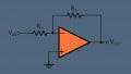
We began with a basic composite voltage amplifier, as follows:

Figure 1. A block diagram of a composite voltage amplifier, which we will reference in this article.
We also learned how to use the rate-of-closure (ROC) technique to assess the stability of a composite amplifier and estimate the phase margin ɸm, as shown below.
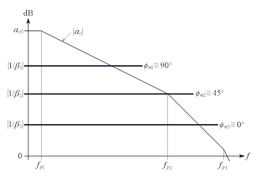
Figure 2. Frequently encountered phase-margin situations
Finally, we discussed one method of increasing an op-amp's output current drive capability: using a voltage buffer.

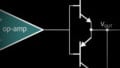
Figure 3. The voltage buffer utilized in the previous article.
Now, we will simulate our buffer in PSpice and utilize it to boost the output current drive of a 741 op-amp.
Voltage Buffer Simulation
We can gain a lot of additional insight by simulating our buffer via PSpice, as depicted in Figure 4.
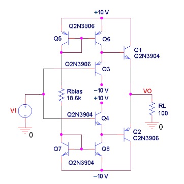
Figure 4. PSpice circuit simulating a buffer loaded with a 100-Ω resistor.
We make the following observations:
- By Equation 3 from the previous article,
\[I_{BIAS} = \frac {(V_{CC}-V_{EBp})-(V_{EE}+ V_{EBn})}{R_{BIAS}}\]
we have IBIAS = 1 mA.
- Performing a DC Sweep of VI from –10 V to +10 V gives the voltage transfer curves of Figure 5.
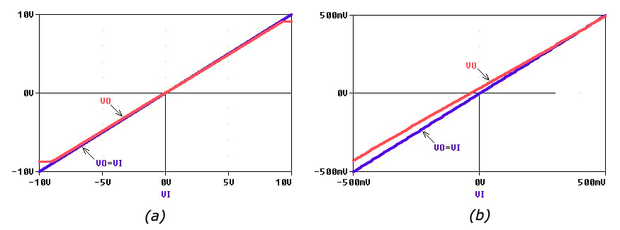
Figure 5. (a) Voltage transfer curve (VTC) of the PSpice circuit of Figure 4. (b) Expanded view near the origin, showing the absence of distortion. For comparison, also the ideal-buffer case VO = 1×VI is shown.
- The slope of the VTC is about 0.9 V/V, that is, about 10% less than the idealized case of 1.0 V/V.
- The VTC is shifted a bit upwards. In fact, performing the Bias Point Analysis in Figure 4 with VI = 0 V gives VO ≅ 72 mV (≠ 0 V). This is due to mismatches between the base-emitter voltage drops of the npn and pnp BJTs Q1 through Q4. For instance, even though Q3 and Q4 draw the same current, we measure their base-emitter voltage drops as VEB3 = 725 mV and VBE4 = 645 mV (≠725 mV).
- The Bias Point Analysis indicates that to achieve VO = 0 we must set VI = –36.3 mV. This is the input offset voltage VOS of the buffer.
- Making VI (in Figure 4) a 1-kHz sine wave with an amplitude of 1.0 V and an offset of –36.3 mV, and then performing the Time Domain Analysis gives the current waveforms of Figure 6(a). It is interesting to observe how Q1 and Q2 alternate in push-pull fashion to generate the undistorted sinusoidal load current IL.
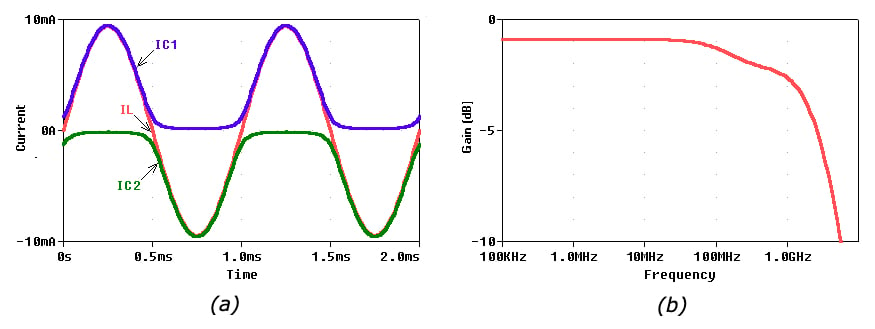
Figure 6. (a) Collector currents IC1 and IC2 of the BJTs Q1 and Q2 of Figure 4, and current IL through the load resistance RL. (b) AC response of the buffer of Figure 4.
- Making VI (in Figure 4) an ac source with an offset of –36.3 mV, and performing the AC Sweep Analysis gives the gain plot of Figure 6b, which indicates a DC value of –0.897 dB (≅ 0.9 V/V) and a –3-dB frequency of about 2 GHz. The buffer is indeed a very fast circuit!
Composite Amplifier Simulation
Let us now use our buffer to boost the output current drive of a 741 op-amp, as shown in Figure 7. The 741 is configured for a closed-loop gain of –2 V/V, so, according to the notation of Figure 1, we have β = R1/(R1 + R2) = 1/3.
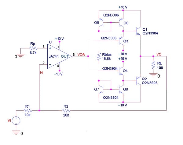
Figure 7. Using the buffer of Figure 4 to boost the output current drive of a 741 op-amp.
Moreover, a1 of Figure 1 is now the 741’s open-loop gain (DC value of 200,000 V/V, bandwidth of 5 Hz, and gain-bandwidth product GBP of 1 MHz) and A2 of Figure 1 is the buffer’s gain (DC value of about 0.9 V/V, and bandwidth of about 2 GHz).
The pole frequency (~2 GHz) introduced by the buffer is much higher than the op-amp’s GBP (~1MHz), so it won’t affect the stability: the circuit is operating in the condition of the 1/β1 curve of Figure 2(a), so we have ɸm ≅ 90°.
The AC Sweep Analysis gives the plot of Figure 8, which reveals a closed-loop gain with a DC value of –2.0 V/V (= 6.02 dB), a bandwidth of 347 kHz, and no peaking whatsoever. (For good measure, place a small capacitor CF in parallel with R2 to combat the op-amp’s inverting-input stray capacitance Cn).
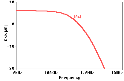
Figure 8. Closed-loop gain of the composite amplifier of Figure 7.
Figure 9(a) shows the input-output sinusoidal waveforms of the composite amplifier of Figure 7, obtained by making VI a 1-kHz sine wave with an amplitude of 4.0 V and an offset of 0 V.
Figure 9. (a) Input-output sinusoidal waveforms of the circuit of Figure 7. (b) A more detailed plot, showing also the output VOA supplied by the op-amp.
We note the following:
- As expected, the circuit gives VO = −2VI.
- With zero input offset, we also get zero output offset. What happened to the buffer’s input offset voltage VOS = –36.3 mV? A look at the more detailed plot of Figure 9(b) reveals that it is the op-amp itself that shifts its VOA by –36.3 mV in order to compensate for VOS.
- There is no distortion in connection with the zero crossings of VOA. This stems from the class AB operation of the buffer’s push-pull stage.
- What about the fact that the buffer has a gain of 0.9 V/V, instead of 1.0 V/V? Again, it is the op-amp that overdrives the buffer by 1/0.9 = 1.11 V/V to compensate for the buffer’s gain loss of 0.9 V/V.
- The above-mentioned downshift and overdrive of VOA corroborate the popular saying: “The op-amp will do its best to drive the voltage difference between its inputs as close as possible to zero.” In the present case, the op-amp achieves this by forcing VO/2 to track –VI.
Another, less obvious, benefit enjoyed by the above composite amplifier is that any self-heating due to the power dissipated by the push-pull stage is confined to the buffer itself, so it does not contribute to the thermal drift of the primary amplifier’s input offset voltage and input bias current.
Voltage buffers are available also in integrated-circuit form. Popular examples are the EL2033, LH0002, LT1010, and OPA633. These devices include also output short-circuit protection circuitry (not shown in Figure 3(b)).
In the next part of this composite amplifier series, we'll focus on achieving faster op-amp dynamics by way of expanding the frequency bandwidth.
Related Content


A nice explanation, and clearly written.
Regarding the commercially available buffers listed whose topologies are very similar to that of the Q1 - Q8 sub-circuit in the article’s Figure 7, I’ve often wondered why the collectors of Q3 and Q4 are not returned to the emitters of Q2 and Q1 respectively. By so cascoding Q3 and Q4, my simulations show that the buffer’s input impedance would be increased by a factor of about 30dB below 1MHz. Granted, this would not make much of a difference in the case of the article’s op amp drive, but it would make the buffer more useful as a wide bandwidth device for use with high input impedance sources.