Facebook
 Google
 GitHub
 Linkedin
How to Boost the Output Current Drive Capability of an Op-Amp
In the first part of this series on composite amplifiers, we'll investigate one method of boosting an op-amp’s output current drive capability.
In Part 1 of this series on composite amplifiers, we investigate how to boost an op-amp’s output current drive capability. This article will present one method of accomplishing this task.
There are applications that could be realized with just a single ideal op-amp, but cannot be realized in practice with just one real-life device because of certain physical limitations. Mercifully, it is often possible to enlist the help of a second amplifier so that the combination of the two, aptly called a composite amplifier, can do what the primary amplifier could not do alone.
Stability Considerations in Composite Amplifiers
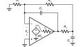
The secondary op-amp is usually placed inside the feedback loop of the primary op-amp, as depicted in Figure 1(a). The phase lag introduced by the secondary device tends to erode the phase margin ɸm of the composite amplifier, so we may have to take suitable frequency compensation measures.
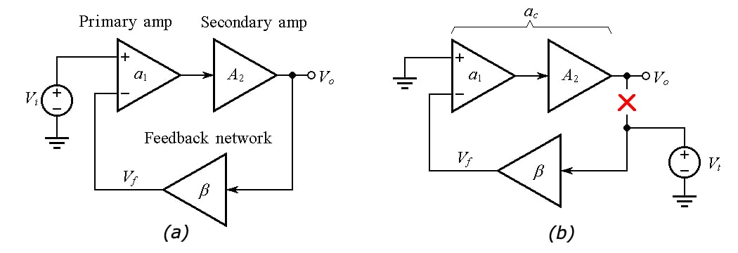
Figure 1. (a) Block diagram of a composite voltage amplifier. (b) Circuit to find the open-loop gain ac and noise gain 1/β of the composite amplifier.
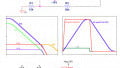
To assess the stability of the composite amplifier, we shall use the rate-of-closure (ROC) technique. This technique requires that we plot
- the overall open-loop gain ac (= a1× A2) of the composite amplifier, along with
- its noise gain 1/β, where β is the feedback factor of the composite amplifier.
Then we refer to Figure 2 to identify the situation at hand and estimate ɸm accordingly.
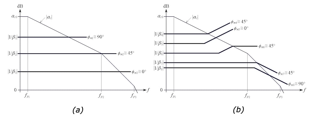
Figure 2. (a) Frequently encountered phase-margin situations with (b) frequency-independent and (b) frequency-dependent noise gain 1/β(jf).
To find ac and 1/β, we break the circuit as in Figure 1(b), where presumably the output impedance of the secondary amplifier is much smaller than the impedance presented by the feedback network. Next, we apply a test voltage Vt , and finally we let
\[a_c = \frac {V_o}{-V_f}\]
Equation 1
and
\[\frac {1}{\beta} = \frac {V_t}{V_f}\]
Equation 2
Boosting the Output Current Drive Capability of an Op-Amp
Most op-amps are designed to provide output currents of not more than a few tens of milli-Amperes. As an example, the venerable 741 op-amp can handle at most 25 mA of output current. Trying to exceed this value activates some internal watchdog circuitry that prevents the actual current from increasing further.
Under this condition, the op-amp will no longer function properly, but at least it will be protected from possible damage due to excessive power dissipation.
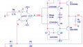
A popular way to boost an op-amp’s output current drive capability is by means of a voltage buffer as exemplified in Figure 3(a).

Figure 3. (a) Using a buffer to boost an op-amp’s output current drive. (b) Detailed buffer schematic.
The function of Q1 is to source (or push) current to the load RL, whereas that of Q2 is to sink (or pull) current out of RL; hence the reason why the Q1-Q2 pair is said to form a push-pull output stage. Transistors Q3 and Q4 serve a dual purpose:
- They provide a Darlington-type function to raise the current gain from the input to the output node.
- Their base-emitter voltage drops are designed to keep Q1 and Q2 already conductive even in the absence of any output load, this being the reason why Q1 and Q2 are also said to form a class AB output stage. Class AB operation prevents the distortion inherent to Class B operation.
For a more detailed analysis, refer to the full-blown schematic of Figure 3(b), where we note the following:
- The Q5-Q6 and the Q7-Q8 pairs form two current mirrors sharing the same bias current IBIAS, where
\[I_{BIAS} = \frac {(V_{CC}-V_{EBp})-(V_{EE}+ V_{EBn})}{R_{BIAS}}\]
Equation 3
- Q6 and Q8 mirror IBIAS and use it to bias Q3 and Q4, respectively. As a consequence, Q3 and Q4 develop the base-emitter voltage drops VEB3 and VBE4.
- In response to VEB3 and VBE4, Q1 and Q2 develop the base-emitter drops VBE1 and VEB2 such that
\[V_{BE1} + V_{EB2} = V_{EB3} + V_{BE4}\]
Equation 4
- In the absence of any load, Q1 and Q2 must draw the same current. In view of Equation 4, the common current drawn by Q1 and Q2 must equal that drawn by Q3 and Q4, which is IBIAS. Consequently, with no load, the collector currents satisfy the condition IC1 = IC2 = IC3 = IC4 = IBIAS.
In the next article, we'll expand this conversation by simulating our voltage buffer in PSpice and utilize that analysis to boost our 741 op-amp's current output drive.
Related Content