 Facebook
 Google
 GitHub
 Linkedin
How to Drive Large Capacitive Loads with an Op-Amp Circuit
Learn more about capacitive load compensation.
Learn more about capacitive load compensation.
There are applications in which an op-amp drives a heavily capacitive load: typical examples are sample-and-hold amplifiers, peak detectors, coaxial drivers, and drivers for certain types of A/D (analog-to-digital) converters.
Capacitive loads have a notorious tendency to destabilize negative-feedback circuits because of the pole formed by the capacitive load with the output resistance of the error amplifier. Being inside the feedback loop, this pole introduces phase lag, which erodes the phase margin of the system, leading to peaking in its AC response, and ringing in its transient response, or even to outright oscillation.
Supporting Information
- Negative Feedback, Part 1: General Structure and Essential Concepts
- Negative Feedback, Part 5: Gain Margin and Phase Margin
- Negative Feedback, Part 9: Breaking the Loop
Before analyzing this source of instability in detail, let us quickly review the basics of circuit stability.
Understanding Circuit Stability
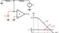
We'll demonstrate the concept of circuit stability and instability with an example noninverting amplifier, shown in Figure 1(a) below.
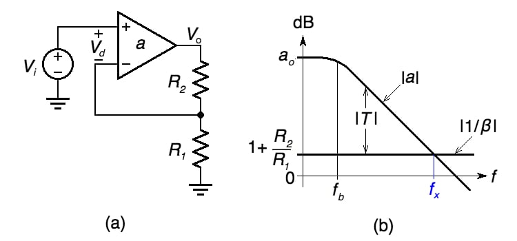
Figure 1. (a) A noninverting amplifier and (b) graphical visualization of its loop gain |T|.
In this example noninverting amplifier, any signal injected at the amplifier’s input port is first magnified by the open-loop gain a and is then attenuated by the feedback factor
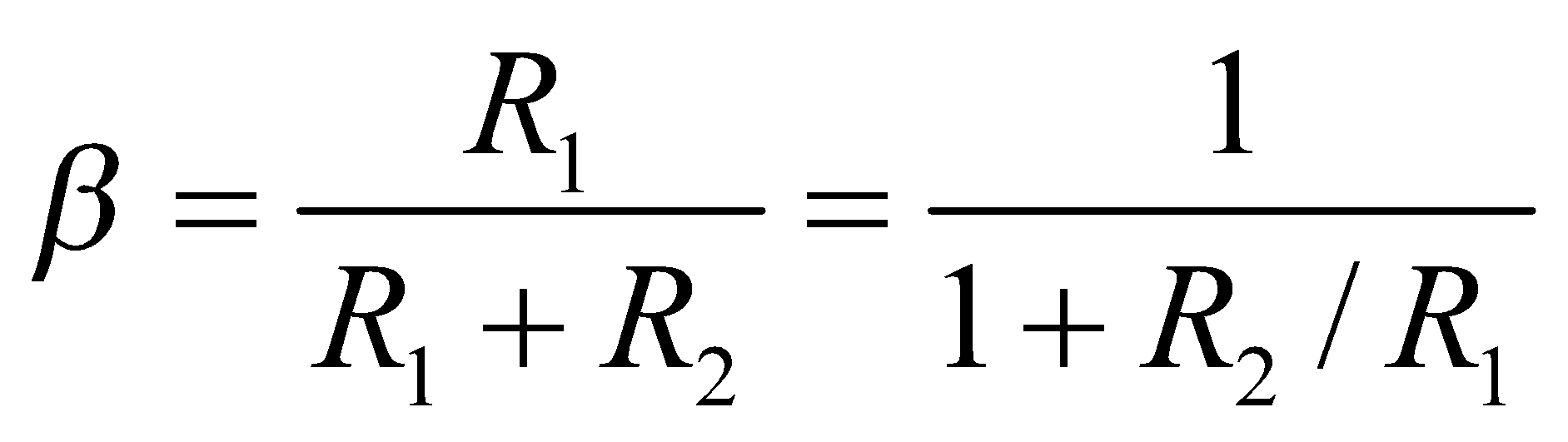
Equation 1
Thus, the overall gain T experienced by the signal in going around the loop, aptly called the loop gain, is
T = aβ
Equation 2
Rewriting as T = a/(1/β), taking the logarithms, and multiplying by 20 to convert to decibels, gives
|T|dB = |a|dB - |1/β|dB
indicating that we can visualize the decibel plot of |T| as the difference between the decibel plots of |a| and |1/β|. This is depicted in Figure 1(b) for the case of a constant gain-bandwidth product op-amp, the most common op-amp type.
The frequency fx at which the two curves intersect, aptly called the crossover frequency, plays an important role because it offers a quantitative indication of circuit stability via the phase margin φm, defined as
φm = 180° + ph[T(jfx)]
Equation 3
where ph[T(jfx)] represents the phase of T at fx,
ph[T(jfx)] = ph[a(jfx)] + ph[β(jfx)| = ph[a(jfx)] – ph[1/β(jfx)|
For the single-pole example shown, ph[1/β] = 0; ph[a] starts out at 0° at DC, drops to –45° at the pole frequency fb, and tends asymptotically to –90° at higher frequencies. By inspection, we have in this case φm ≅ 180° – 90° = 90°. The AC and transient responses of this circuit will be similar to those of an ordinary R-C network.
However, should φm get reduced for some reason, then the AC response will exhibit peaking for φm ≤ 65.5°, and the transient response will exhibit ringing for φm ≤ 76.3°. For φm = 45°, the circuit exhibits a peaking of 2.4 dB, and ringing with an overshoot of 23%.
Capacitively Loaded Op Amp Circuit
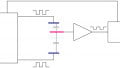
We now turn our attention to the capacitively loaded circuit of Figure 2.
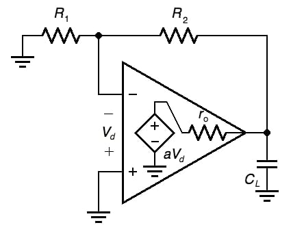
Figure 2. A capacitively loaded op-amp circuit
This figure explicitly shows the output resistance ro internal to the op-amp. A well-designed circuit will have R1 + R2 >> ro, so we can ignore loading of the output node by the feedback network and say that ro and CL establish a pole frequency of

Equation 4
We can examine the effect of this pole from two different but equivalent viewpoints, for which we will look to Figure 3 for demonstration.
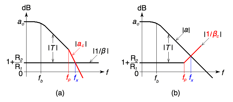
Figure 3. Combining the ro-CL network (a) with the amplifier, and (b) with the feedback network.
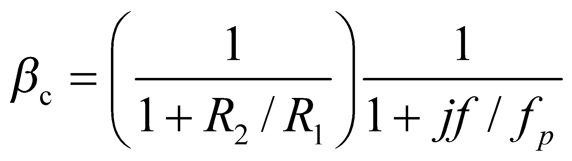
- In Figure 3(a) we combine the ro-CL network with the amplifier itself, so from the viewpoint of the feedback network R1-R2, this combination acts as a composite amplifier with open-loop gain
Clearly, the loop gain T has now two pole frequencies, fb and fp, each contributing to ph[T(jfx)] a phase shift approaching –90°, so the circuit will exhibit a phase margin approaching zero, with generally intolerable peaking and ringing.
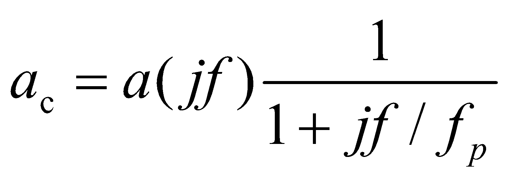
- In Figure 3(b), we combine the ro-CL network with the feedback network itself, so from the viewpoint of the amplifier’s dependent source, this combination appears to have the composite feedback factor
Note that as we plot |1/βc|, the pole frequency fp becomes a de facto zero frequency. Considering that we now have ph[T(jfx)] = ph[a(jfx)] – ph[1/βc(jfx)], with ph[a(jfx)] approaching –90° and ph[1/βc(jfx)] approaching +90°, we still have a system with a phase margin approaching zero.
Frequency Compensation
For the circuit to function properly we need to modify its loop gain so as to restore an acceptable phase margin—a process called frequency compensation. The popular scheme of Figure 4 utilizes a small series resistance Rs to decouple the amplifier’s output pin from CL, and a small feedback capacitance Cf to provide a high-frequency bypass from the output pin back to the inverting input pin, adjusted so as to neutralize the phase lag due to fp.
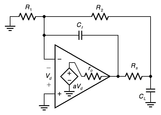
Figure 4. A popular frequency-compensation scheme for the circuit of Figure 2.
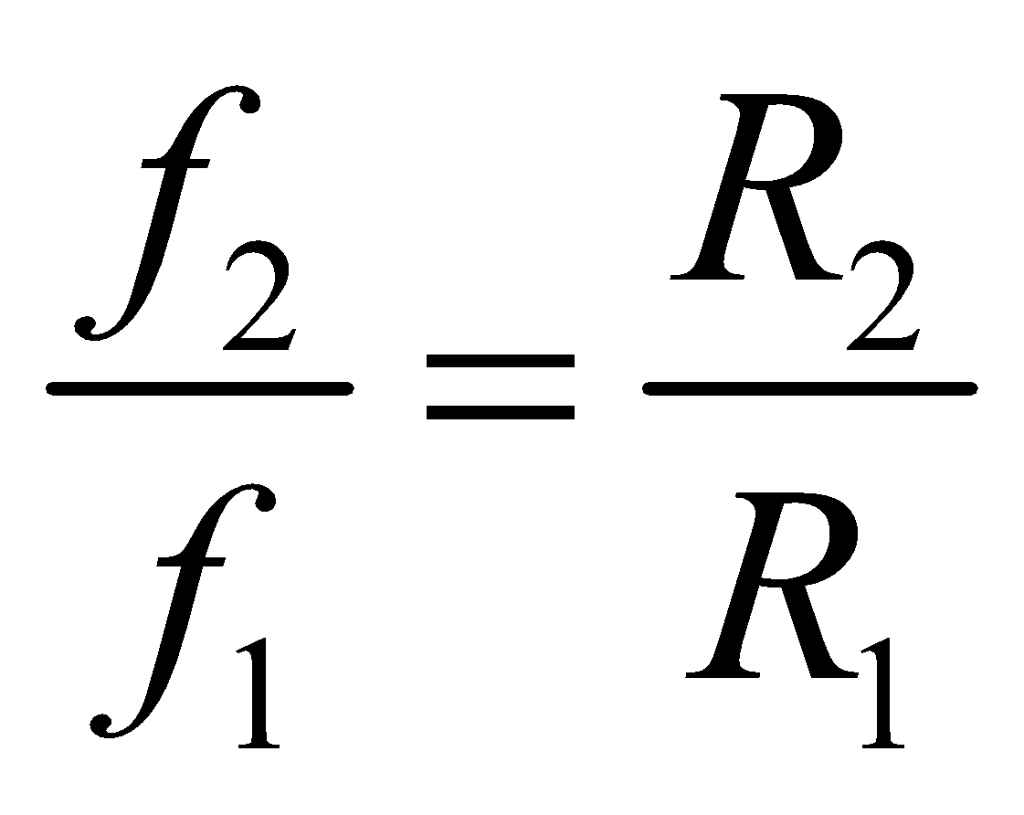
The objective here is to bend downward the rising portion of the |1/βc| curve of Figure 2(b) so as to make it look like the |1/β| curve of Figure 1(b), which we know to provide a phase margin of about 90°. To this end, we need to impose two conditions:
- The high-frequency asymptote must equal the low-frequency asymptote, the latter being 1 + R2/R1. Considering that at sufficiently high frequencies both capacitors act as short circuits, it is apparent that the R1-R2 network is disabled, so the high-frequency asymptote becomes 1 + ro/Rs (recall that we are assuming a well-designed circuit with negligible loading by the R1-R2 network). For the asymptotes to be equal, we thus need 1 + ro/Rs = 1 + R2/R1, or
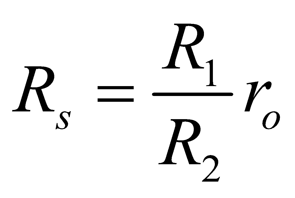
Equation 5
- With Rs in place, the in-loop pole frequency changes to

Also, Cf forms a high-pass C-R network with the combination R1||R2 (again we are assuming a well-designed op-amp circuit with R1||R2 >> ro||Rs), so its pole frequency is
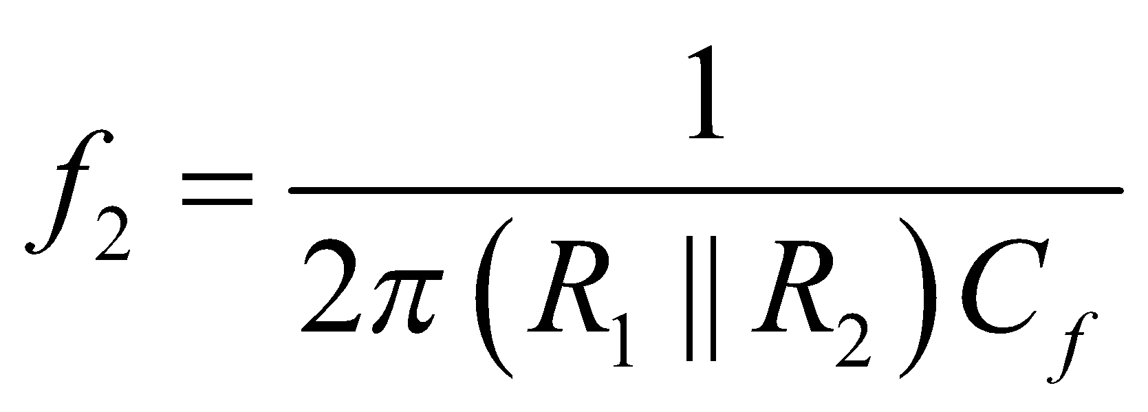
We wish the phase lead introduced by Cf to neutralize the phase lag due to CL. This we achieve by imposing [1]
Substituting the above expressions for f1 and f2 and solving for Cf gives

Equation 6
Moreover, the –3 dB frequency of the closed-loop gain is [1]

Equation 7
Verification Via PSpice
We wish to verify the above considerations using the example of Figure 5, having R2 = 2R1 = 20 kΩ and CL = 100 nF. PSpice’s 741 macromodel has ro = 50 Ω, so we use Equations 5 and 6 (shown above) to calculate Rs = 25 Ω and Cf = 562.5 pF.

Figure 5. PSpice circuit to plot the open-loop gain a and 1/β.
Let us first check that compensation does indeed flatten out the 1/β curve. In order to visualize the situation from the viewpoint of the op-amp’s internal source, we need to bring the op-amp’s output resistance ro outside, and subject it to a test voltage Vt, as shown. Running the circuit first with Rs = 0 and Cf = 0, we get the rising 1/β curve of Figure 6, which crosses the a curve at 100.4 kHz, where we find ph[a] ≅ –93.3° and ph[1/β] ≅ +72.4°. Consequently, ph[T] = ph[a] – ph[1/β] = –93.3° – (+73.4°) = –165.7°, so Equation 3 gives φm = 14.3°, a recipe for intolerable peaking and ringing, as shown in Figure 8 (below).
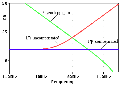
Figure 6. Plots obtained using the circuit of Figure 5. Here, a = V(OA)/V(T), and 1/β = V(T)/V(N).
Next, we re-run PSpice with Rs and Cf in place, as shown, and we get the flat 1/β curve, which crosses the a curve at 326.2 kHz, where ph[T] = ph[a] – ph[1/β] = –100.7° – 0° = –100.7°, so now φm = 180° – 100.7° = 79.3°, a much better margin. The compensated responses are shown in Figure 8. Equation 7 predicts a –3 dB frequency of 21.2 kHz, which is close to the measured value of 21.1 kHz. Note that the closed-loop AC response has two pole frequencies, 21.2 kHz, and 326.2 kHz.
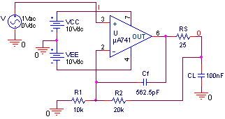
Figure 7. PSpice circuit to plot the closed-loop AC response. The closed-loop transient response is obtained by changing the input source to a 1.0-V step.
![]()
Figure 8. Closed-loop (a) AC responses and (b) transient responses obtained using the uncompensated and compensated versions of the simulation circuit.
Conclusion
This article has discussed the way in which a large capacitive load can reduce the stability of a negative-feedback amplifier. Compensation can be achieved by the addition of a resistor and capacitor, and the article presents a method of calculating appropriate values for these components.
It should be pointed out that the op-amp’s output impedance, denoted by ro, is not always a well-known parameter; moreover, at high frequencies it may become reactive. Consequently, the above equations should be taken as a starting point, after which the designer may find it necessary to tweak the initial values to optimize the circuit for the particular application at hand.
References
[1] Design with Operational Amplifiers and Analog Integrated Circuits, 4th Edition by Dr. Sergio Franco
Related Content


Very useful circuit configuration, I use it all the time. I have a different way of looking at stability. As a Filter Wizard, I see filters in many circuits; this is basically a 2nd order filter circuit. A simple analysis will give the transfer function, with has a pole frequency and a pole Q. “Simply” solve for the Q and frequency that you think is appropriate for the application. Particularly appropriate when you are using this as a regulator circuit, it its output impedance versus frequency is important (as in audio).
Hi Sergio. I have a question. The loop gain of the non-inverting circuit in fig. 1(a): Wouldn’t it be just beta? The open-loop gain, ‘a’ doesn’t appear at all when this feedback is applied.