 Facebook
 Google
 GitHub
 Linkedin
Input Capacitance in Analog Circuits: How to Compensate for Input Capacitance of Op-Amps
Learn about the effect of input parasitic capacitance and how to compensate for it in analog circuit design.
Learn about the effect of parasitic capacitance at the input and how to compensate for it in analog circuit design.
Most internally compensated op-amps are intended for stable operation at any frequency-independent closed-loop gain, including unity gain.
In practice, the presence of capacitances, whether intentional or parasitic, tend to destabilize the circuit and may require additional compensation measures by the user to restore an acceptable phase margin.
Examples of intentional capacitance at the output are found in sample-and-hold circuits, peak detectors, and voltage-reference boosters with output capacitive bypass. (For capacitive load compensation, refer to my article on how to drive large capacitive loads with an op-amp circuit.)
This article will discuss the effect of parasitic (or stray) capacitances at the input, especially at the inverting input.
Types of Input Capacitance
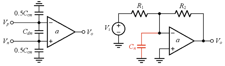
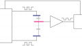
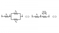
All op-amps exhibit a differential-mode input capacitance Cdm and a common-mode (with the inputs tied together) input capacitance Ccm. These are the capacitances exhibited by the transistors of the input stage, and also by the input protection diodes, if present. (Even though Cdm and Ccm are internal to the op-amp, we show them externally for better visualization.)
In a physical circuit, additional capacitances come into play externally, such as the stray capacitances of the resistors, of their leads, and of the printed circuit traces.
In the amplifier example of Figure 1b, all parasitics associated with the inverting input have been lumped together into a single equivalent capacitance Cn.
(a) (b)
Figure 1. (a) The stray input capacitances of an op-amp. (b) Lumping together all parasitics associated with the inverting input as a single capacitance Cn.
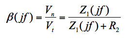
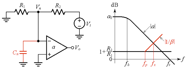
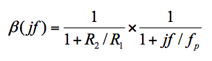
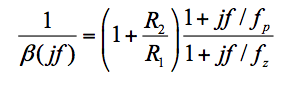
Let's investigate the effect of Cn upon the stability of the circuit via the rate-of-closure (ROC). To this end, we set the input source to zero, break the loop as in Figure 2a (below), apply a test voltage Vt, and calculate the feedback factor ß(jf) as
Equation 1
(a) (b)
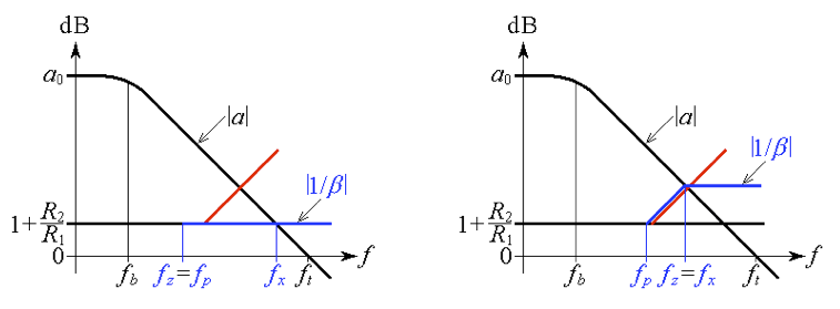
Figure 2. (a) Finding the feedback factor ß(jf). (b) Rate-of-closure (ROC) approaching 40 dB/dec.
where
Equation 2
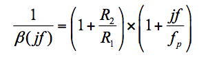
Substituting into Equation (1) we obtain, after some algebraic manipulation,
Equation 3
where
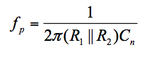
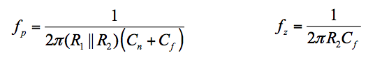
Equation 4
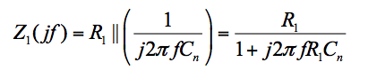
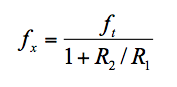
If we focus on the physical meaning of Equation (4), we see that Cn and the resistance R1||R2 presented to it by the surrounding circuitry establish a pole frequency within the feedback loop. Consequently, a signal traveling around the loop will have to contend with two poles, one due to the op-amp and the other due to Cn, with the risk of a phase shift approaching 180° and thus jeopardizing circuit stability.
We can better visualize this in Figure 2b, which shows the plots of the open-loop gain |a| and the reciprocal of the feedback factor |1/ß(jf)|, where
Equation 5
The pole frequency fp of ß(jf) is a zero frequency of 1/ß(jf), indicating that the |1/ß(jf)| curve starts to rise at fp. If fp is low enough compared to the crossover frequency fx, the rate-of-closure will approach 40 dB/dec, indicating a phase margin approaching zero.
How to Mitigate Phase Lag Due to Single Equivalent Capacitance
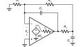
A common cure for combating the phase lag due to Cn is to introduce phase lead by means of a feedback capacitance Cf across R2, as depicted in Figure 3.
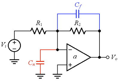
Figure 3. Exploiting the phase lead introduced by Cf to combat the phase lag due to Cn.
Equation (1) still holds, provided we replace R2 with Z2(jf) = R2||(1/j2πƒCf). This gives, after some algebraic manipulation,
Equation 6
where
Equation 7
What is important to note here is that the presence of feedback capacitance creates a zero frequency fz for ß(jf), while also lowering the existing pole frequency fp somewhat (recall that a pole/zero for ß becomes a zero/pole for 1/ß).
How to Select Feedback Capacitance
There are two common approaches to the selection of Cf :
- fz = fp
- fz = fx
fz = fp
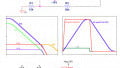
Impose fz = fp so that the zero cancels out the pole in Equation (6), giving 1/ß = 1 + R2 /R1 throughout, as depicted in Figure 4a.
(a) (b)
Figure 4. Imposing (a) fz = fp for a phase margin ɸm ≈ 90°, or (b) fz = fx for ɸm ≈ 45°.
Equating fz and fp of Equation (7) gives, after simplification,
Equation 8
This choice of Cf results in a phase margin of about 90°. To find the crossover frequency fx we exploit the constancy of the gain-bandwidth product on the |a| curve to write (1 + R2 /R1) × fx = ft, so
Equation 9
Note that the closed-loop gain has two pole frequencies, fz and fx, with its –3-dB frequency close to fz.
fz = fx
Impose fz = fx, as depicted in Figure 4b, for a phase margin of about 45°. The closed-loop gain will now have a higher –3-dB frequency, but at the price of some peaking and ringing.
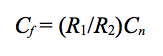
To find the required Cf, we must first find fx. Considering that the high-frequency asymptote of 1/ß is 1 + Cn /Cf, we exploit once again the constancy of the gain-bandwidth product on the |a| curve to write (1 + Cn /Cf) × fx = ft, so fx = ft /(1 + Cn /Cf).
Imposing fz = fx means imposing 1/(2πR2Cf) = ft /(1 + Cn /Cf). Anticipating Cn /Cf >> 1, we approximate 1/(2πR2Cf) ≈ ft /(Cn /Cf) = ftCf /Cn, which we solve for Cf to get
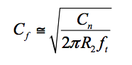
Equation 10
Note that the closed-loop gain now has two coincident pole frequencies at fx.
Verification via PSpice
We wish to verify the above considerations by means of the circuit of Figure 5, which uses a constant gain-bandwidth op-amp with ft = 10 MHz.
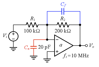
Figure 5. An inverting amplifier example with a gain of –2 V/V.
Now let's take a look at Figure 6:
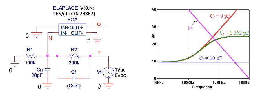
Figure 6. PSpice circuit to plot |a| and |1/ß|. (b) The |1/ß| curves for different values of Cf.
With reference to Figure 6, we make the following considerations:
- Without compensation (Cf = 0), the crossover frequency is measured as fx ≈ 625 kHz, and the phase angles are measured as ph[a(jfx)] ≈ –90° and ph[1/ß(jfx)] ≈ 79.2°, so
ɸm = 180° + ph[a(jfx)] – ph[1/ß(jfx)] ≈ 180 – 90 –79.2 = 10.8°
Equation 11
indicating a circuit on the verge of oscillation.
- For a phase margin of ɸm ≈ 90°, we use Equation (8) to get Cf = 10 pF. By Equation (9) we have fx ≈ 3.33 MHz. As shown in Figure 6b, we now have
ɸm ≈ 90°.
- For ɸm ≈ 45° we use Equation (10) to get Cf = 1.262 pF. Using PSpice’s cursor, we now measure fx = 762.1 kHz and ɸm = 58.8°. This is better than the anticipated 45°. To see why, use Equation (7) to calculate fp = 112.28 kHz and fz = 630.57 kHz, and then use Equation (6) to calculate
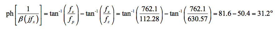
Then, proceed in the manner of Equation (11) to find ɸm = 180°– 90 –31.2 = 58.8°.
Closed-Loop ac Responses
Shown in Figure 7 are the closed-loop ac responses for the three cases under consideration.
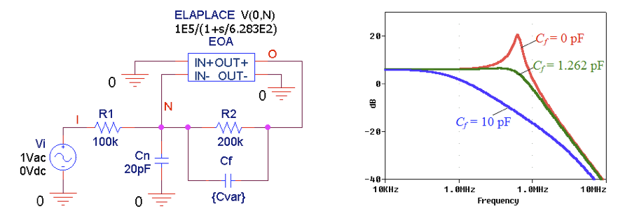
Figure 7. Using PSpice to plot the closed-loop ac responses for different values of Cf.
As expected, the uncompensated response exhibits quite a bit of peaking. Peaking is almost unnoticeable for Cf = 1.262 pF, in which case the response exhibits a pair of coincident pole frequencies at about 762 kHz. The response for Cf = 10 pF is the most sluggish, this being the price we pay for a large phase margin.
As mentioned, this response contains two pole frequencies, namely, fz and fx.
Shown in Figure 8 are the step responses, which, after the discussion of the ac responses, should be self-explanatory.
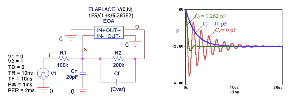
Figure 8. Using PSpice to plot the closed-loop step responses for different values of Cf.
Are Stray Capacitances Always a Bad Thing?
It is worth pointing out that the stray capacitances, though generally undesirable, are not necessarily always a curse.
Suppose the circuit under consideration had been implemented with R1 = 1.0 kΩ and R2 = 2.0 kΩ, that is, with values scaled down by two decades, while still ensuring the same closed-loop gain of –2 V/V. Then, according to Equation (4), fp would scale up by two decades, to a value well beyond fx so that compensation would be unnecessary.
The price for this advantage would be, of course, increased power dissipation by the lower resistances. As an exercise, you can find out how low one would need to scale the resistances in order to achieve a phase margin of 60° without compensation.
Related Content


But, I want a simple circuit to amplify an AC signal. I tried and tried but didn’t know how to do it.
I didn’t actually use any capacitors. Then I used caps in series with input and output but also didn’t work.
There’s something I’m missing ..
For the case of fz=fp, I still don’t quite understand the why BW of closed loop system is closed to fz. why the BW cannot be equal to ft*beta if considering accurately matching? Even accurate matching cannot be achieved across PVT, should it just be a pole-zero or zero pole doublet? Why the BW will drop so significantly?
Yes, you do have a pole freq at beta*ft. You also have another at 1/(2*pi*R2*Cf). You’d have this second pole EVEN IF the op amp were IDEAL.