Facebook
 Google
 GitHub
 Linkedin
Learn Analog Circuits: Types and Applications of Current Mirrors
The current mirror is an important analog building block that finds application in such diverse areas as DC biasing and current-mode signal processing.
Learn more about analog design in this introduction to the current mirror, including how this circuit is implemented in analog ICs.
The current mirror is an important analog building block that finds application in such diverse areas as DC biasing and current-mode signal processing. This block comes in various incarnations, which we will investigate below:
- Basic mirror
- Mirror with beta helper
- Widlar current source
- Wilson mirror
We'll begin by looking at some basic characteristics of a bipolar junction transistor (BJT).
Background: BJT Characteristics
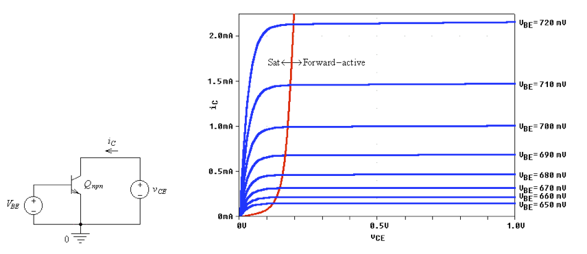
To set the background, consider Figure 1, which shows the iC-vCE characteristics of an NPN BJT for different base-emitter voltage drives VBE.
(a) (b)
Figure 1. Using PSpice to display the iC-vCE characteristics of an NPN BJT. For vCE < 0.2 V the BJT is in saturation (Sat), whereas for vCE ≥ 0.2 V it is operating in the forward-active (FA) region.
We observe that, for vCE ≥ 0.2 V, all curves are essentially flat, indicating the BJT’s ability to sink current independently of the collector voltage (so long as this voltage is prevented from dropping below about 0.2 V). Even though VBE is incremented in equal 10 mV steps, iC increases in geometric fashion. In fact, in the forward-active (FA) region, iC is related to vBE exponentially as
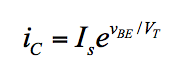
Equation 1
where Is is a scaling factor called the saturation current, and VT is another scaling factor called the thermal voltage because it is proportional to absolute temperature T. For a low-power BJT, Is is typically in the femtoampere range (1 fA = 10–15 A).
Moreover, VT = 26 mV at room temperature. Figure 2a shows the PSpice plot of Equation (1) for a BJT with Is = 2 fA (this value has been chosen so that with vBE = 700 mV the BJT gives exactly iC = 1.0 mA).
(a) (b)
Figure 2. Using PSpice to plot (a) iC vs. vBE and (b) vBE vs. iC.
The inverse of Equation (1) is
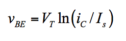
Equation 2
To plot vBE as a function of iC via PSpice, we connect the base and collector terminals together to operate the BJT in what is called the diode mode, and then we apply a test current iT, as shown in Figure 2b.
Basic Current Mirror
The basic mirror, shown in Figure 3a, consists of a pair of matched BJTs fabricated (or mounted) in close proximity to each other so that their characteristics (Is and VT) track each other with temperature and time.
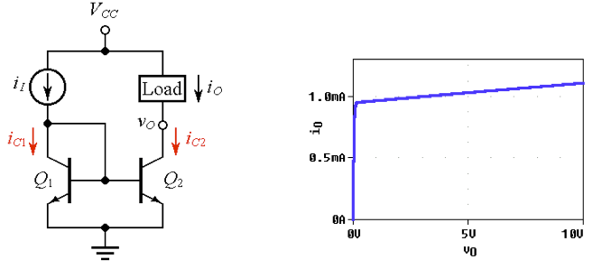
(a) (b)
Figure 3. (a) Basic current mirror, and (b) its iO vs. vO characteristic for iI = 1 mA and VCC = 10 V.
Assuming negligible base currents, we note that diode-connected Q1 responds to the input current iI by developing a voltage drop vBE according to Equation (2) shown above.
Since Q2 is experiencing the same vBE as Q1, we must have iC2 = iC1, by Equation (1), so Q2 mirrors Q1. Assuming negligible base currents, we thus have iO = iI.
Compared to Figure 1b, the expanded view of Figure 3b indicates that the curve in the FA region exhibits a nonzero slope. This stems from the so-called Early Effect [1], as a consequence of which the projections of all curves meet at a common point on the negative axis called the Early Voltage VA, as shown in Figure 4.
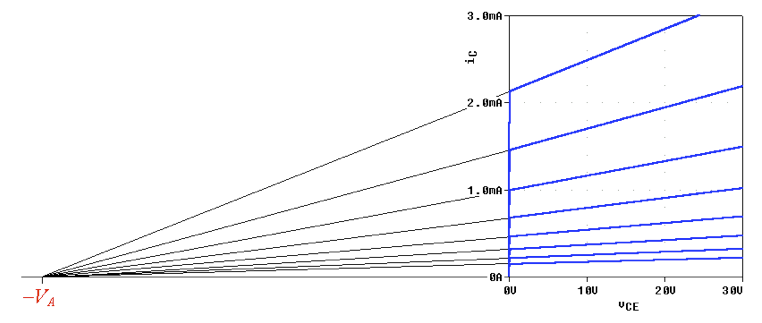
Figure 4. Expanded view of Figure 1b, illustrating the consequences of the Early Effect.
The slope of an iC curve in the FA region is denoted as 1/ro, the reciprocal of resistance. Applying simple geometric reasoning to Figure 4, we have the slope (= 1/ro) ≈ IC / VA, or
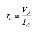
Equation 3
where IC represents the current at the left edge of the FA region.
The PSpice example shown uses VA = 60 V, so for IC = 1 mA we have ro ≈ 60/10–3 = 60 kΩ. This means that the Norton equivalent seen by the load is a 1 mA current sink with a parallel resistance of 60 kΩ. For every volt increase in vO, ro is responsible for an increase in iO of (1 V)/(60 kΩ) = 16.7 µA.
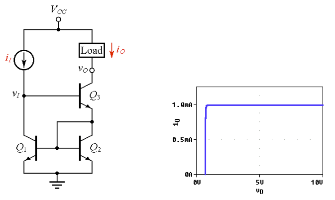
Current Mirror with Beta Helper
We now wish to take a closer look at the base currents of the basic mirror of Figure 3a. It is well known that a BJT’s base current iB is related to the collector current iC as iB = iC / ß, where ß is the BJT’s current gain. Typically, ß ≈ 100, though integrated-circuit BJTs may have ß ≈ 250. With reference to Figure 3a, KCL at Q1’s collector node implies iI = iC1 + iB1 + iB2 ≈ iC1 + 2iB1 = iC1 +2iC1/ß = iC1(1 + 2/ß), or
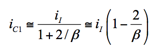
Equation 4
indicating that iC1 (and hence iC2, by mirror action) will be a bit less than iI. For instance, with ß = 100, iC1 and thus also iO (= iC2 = iC1) will be about 98% of iI. Should this error be intolerable, we can enlist the help of a third BJT Q3 to supply iB1 and iB2 in the manner of Figure 5a.
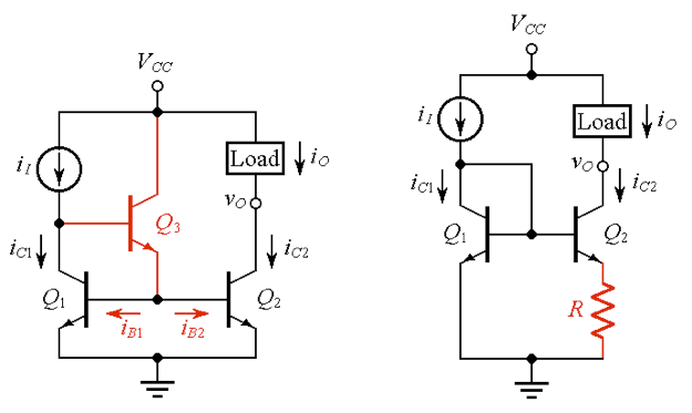
(a) (b)
Figure 5. (a) Current mirror with beta helper, and (b) Widlar current source.
This reduces the error current at Q1’s collector node by a factor of about ß, so Equation (4) still holds, but with ß replaced by ß2.
Widlar Current Source
In DC biasing applications it is often necessary to synthesize a current iO << iI. The circuit of Figure 5b, named for its inventor Bob Widlar, achieves this goal by means of a resistor R in series with Q2 to reduce Q2’s base-emitter voltage drop as
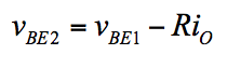
Equation 5
In this connection, it helps to remember the following rules of thumb so dear to practicing engineers:
- To raise (lower) iC by an octave, you need to raise (lower) vBE by 18 mV (because e±18/26 ≈ 2±1).
- To raise (lower) iC by a decade, you need to raise (lower) vBE by 60 mV (because e±60/26 ≈ 10±1).
As an example, suppose we have iI = 1 mA (= 1,000 µA) and we want iO = 20 µA. We can think of 20 as the result of dividing 1,000 by 10 to get 100, dividing 100 by 10 to get 10, and then multiplying 10 by 2 to get 20. So, R must drop (60 + 60 –18) mV = 102 mV. Then, R = (102 mV)/(20 µA) = 5.1 kΩ.
Wilson Current Mirror
There are applications in which it is desirable that a current mirror (a) be exempt from the beta-error of Equation (4), and (b) exhibit a much higher output resistance than the ro of Equation (3), so that it can closely approximate an ideal current source or sink. The mirror of Figure 6a, named for its inventor G. R. Wilson, achieves both objectives with just one additional transistor Q3 (two birds with one stone). This elegant circuit can be analyzed systematically [1], but here we shall limit ourselves to an intuitive discussion.
(a) (b)
Figure 6. (a) Wilson current mirror, and (b) its iO vs. vO characteristic for iI = 1 mA and VCC = 10 V.
We note that Q3 carries the same current as Q2 because they are in series, and Q1, in turn, mirrors the current of Q2, so, the left and right halves of the circuit carry identical currents. This is corroborated by the fact the Q3 draws its base current from the left half, whereas Q1 draws its base current from the right half, in a give-and-take fashion. (A systematic analysis [1] predicts an error of the type of the beta helper.)
Now, if we attempt to raise vO by, say, 1 V, the Early Effect would cause iC3 to increase by (1 V)/ro. This would cause an increase in vBE2, by Equation (2), and this, in turn, would cause an increase in iC1, by Equation (1). Having become a bit more conductive, Q1 would be letting less base current into Q3, forcing the latter to conduct a bit less. In words, any attempt to raise iC3 is met by a reaction that tends to nullify such an attempt. In fact, this is negative feedback! (A systematic analysis [1] predicts a Norton resistance of about ßro/2.) The flatness of the iO curve of Figure 6b confirms the excellent characteristic of the Wilson mirror!
Current Mirrors at Work
It can be fun to look at integrated-circuit schematics and identify the presence and purpose of current mirrors (CMs). For instance, turning to the 741 op-amp of Figure 7, we identify the following CMs:
- The trio Q5 - Q6 - Q7 is a basic CM with beta helper. This CM forms an active load for the differential input stage made up of the left half (Q1 - Q3) and right half (Q2 - Q4). Ideally, the two halves should be perfectly matched, but in practice there may be some mismatch, resulting in an input offset voltage VOS. The emitters of Q5 and Q6 are equipped with 1 kΩ resistors to allow for the creation of an externally induced imbalance equal but opposite to the imbalance of the left and right halves, so as to null VOS. (For the procedure to null the offset voltage VOS, please refer to the fifth figure of this page in the AAC textbook.)
- The pair Q10 - Q11 is a Widlar current sink. The bias current for diode-connected Q11 is established by R5, which is actually a dual-purpose component because it also biases diode-connected Q12.
- The basic CM Q12 - Q13 is designed to source two currents independently, one to provide an active load function for common-emitter amplifier Q17, and the other to bias the circuitry of the output stage. The current entering Q13’s emitter is steered separately by Q13’s two collectors, in percentages determined by the collector areas.
- The pair Q8 - Q9 forms yet another basic CM, which, in connection with the Widlar sink Q10 - Q11, is designed to provide the DC bias current for the two halves of the input stage.
- Can you identify other CMs? Yes indeed, it’s the pair Q23 - Q24. Under normal operating conditions, these BJTs are off because Q21 is off. However, should an overload condition arise at the output, Q21 will go on, turning on also Q24. By mirror action, Q23 will go on and starve Q16 of base current to limit the power dissipated by the output stage.
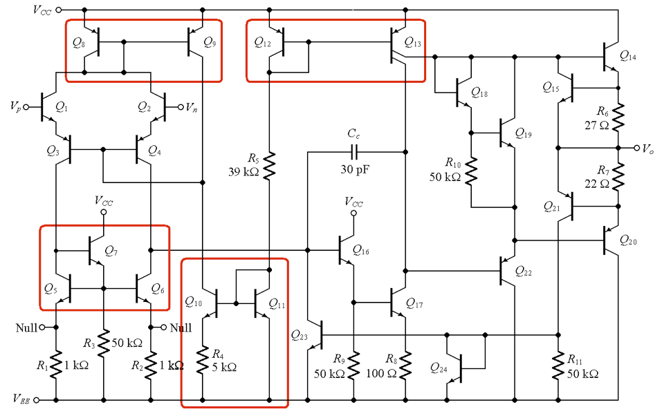
Figure 7. Circuit schematic of the 741 op-amp (courtesy of Fairchild Semiconductor Corporation).
Next, let us look at the CFA of Figure 8.
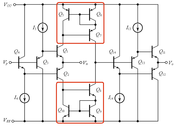
Figure 8. Circuit schematic of a current-feedback amplifier (CFA).
This circuit uses a pair of Wilson CMs, Q5 - Q6 - Q7 and Q8 - Q9 - Q10, to replicate, respectively, the collector currents of Q1 and Q2 and provide their difference at the common base terminals of Q13 and Q14. In a way, the upper CM acts as an active load for the lower CM, just as the lower CM acts as an active load for the upper CM. Furthermore, the DC biasing circuitry consists of the current sources I3 and I13, and the current sinks I4 and I14, which are shown in symbolic form for simplicity. But, if we were to look at a more detailed schematic, we would find that also these sources and sinks are implemented in CM form.
Conclusion
This article briefly reviewed BJT operation, then it explored four types of BJT current mirrors: the basic mirror, the mirror with beta helper, the Widlar current source, and the Wilson mirror. In the final section, we saw some examples of how current mirrors are incorporated into analog integrated circuits.
Current mirrors can also be implemented using CMOS technology. AAC’s article entitled The Basic MOSFET Constant-Current Source is a good place to start if you want to learn about the CMOS version of the current mirror.
References
[1] http://online.sfsu.edu/sfranco/BookAnalog/AnalogJacket.pdf
Related Content