 Facebook
 Google
 GitHub
 Linkedin
Op-Amp Practical Considerations
Real operational amplifiers have some imperfections compared to an “ideal” model. A real device deviates from a perfect difference amplifier. One minus one may not be zero. It may have have an offset like an analog meter which is not zeroed. The inputs may draw current. The characteristics may drift with age and temperature. Gain may be reduced at high frequencies, and phase may shift from input to output. These imperfection may cause no noticable errors in some applications, unacceptable errors in others. In some cases these errors may be compensated for. Sometimes a higher quality, higher cost device is required.
Common-Mode Gain
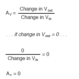
As stated before, an ideal differential amplifier only amplifies the voltage difference between its two inputs. If the two inputs of a differential amplifier were to be shorted together (thus ensuring zero potential difference between them), there should be no change in output voltage for any amount of voltage applied between those two shorted inputs and ground:
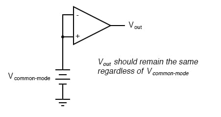
Voltage that is common between either of the inputs and ground, as “Vcommon-mode” is in this case, is called common-mode voltage. As we vary this common voltage, the perfect differential amplifier’s output voltage should hold absolutely steady (no change in output for any arbitrary change in common-mode input). This translates to a common-mode voltage gain of zero.
The operational amplifier, being a differential amplifier with high differential gain, would ideally have zero common-mode gain as well. In real life, however, this is not easily attained. Thus, common-mode voltages will invariably have some effect on the op-amp’s output voltage.
The performance of a real op-amp in this regard is most commonly measured in terms of its differential voltage gain (how much it amplifies the difference between two input voltages) versus its common-mode voltage gain (how much it amplifies a common-mode voltage). The ratio of the former to the latter is called the common-mode rejection ratio, abbreviated as CMRR:

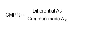
An ideal op-amp, with zero common-mode gain would have an infinite CMRR. Real op-amps have high CMRRs, the ubiquitous 741 having something around 70 dB, which works out to a little over 3,000 in terms of a ratio.
Because the common mode rejection ratio in a typical op-amp is so high, common-mode gain is usually not a great concern in circuits where the op-amp is being used with negative feedback. If the common-mode input voltage of an amplifier circuit were to suddenly change, thus producing a corresponding change in the output due to common-mode gain, that change in output would be quickly corrected as negative feedback and differential gain (being much greater than common-mode gain) worked to bring the system back to equilibrium. Sure enough, a change might be seen at the output, but it would be a lot smaller than what you might expect.
A consideration to keep in mind, though, is common-mode gain in differential op-amp circuits such as instrumentation amplifiers. Outside of the op-amp’s sealed package and extremely high differential gain, we may find common-mode gain introduced by an imbalance of resistor values. To demonstrate this, we’ll run a SPICE analysis on an instrumentation amplifier with inputs shorted together (no differential voltage), imposing a common-mode voltage to see what happens. First, we’ll run the analysis showing the output voltage of a perfectly balanced circuit. We should expect to see no change in output voltage as the common-mode voltage changes:
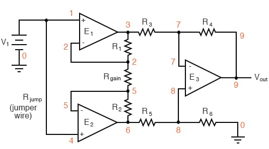
instrumentation amplifier v1 1 0 rin1 1 0 9e12 rjump 1 4 1e-12 rin2 4 0 9e12 e1 3 0 1 2 999k e2 6 0 4 5 999k e3 9 0 8 7 999k rload 9 0 10k r1 2 3 10k rgain 2 5 10k r2 5 6 10k r3 3 7 10k r4 7 9 10k r5 6 8 10k r6 8 0 10k .dc v1 0 10 1 .print dc v(9) .end
v1 v(9) 0.000E+00 0.000E+00 1.000E+00 1.355E-16 2.000E+00 2.710E-16 3.000E+00 0.000E+00 As you can see, the output voltage v(9) 4.000E+00 5.421E-16 hardly changes at all for a common-mode 5.000E+00 0.000E+00 input voltage (v1) that sweeps from 0 6.000E+00 0.000E+00 to 10 volts. 7.000E+00 0.000E+00 8.000E+00 1.084E-15 9.000E+00 -1.084E-15 1.000E+01 0.000E+00
Aside from very small deviations (actually due to quirks of SPICE rather than real behavior of the circuit), the output remains stable where it should be: at 0 volts, with zero input voltage differential. However, let’s introduce a resistor imbalance in the circuit, increasing the value of R5 from 10,000 Ω to 10,500 Ω, and see what happens (the netlist has been omitted for brevity—the only thing altered is the value of R5):
v1 v(9) 0.000E+00 0.000E+00 1.000E+00 -2.439E-02 2.000E+00 -4.878E-02 3.000E+00 -7.317E-02 This time we see a significant variation 4.000E+00 -9.756E-02 (from 0 to 0.2439 volts) in output voltage 5.000E+00 -1.220E-01 as the common-mode input voltage sweeps 6.000E+00 -1.463E-01 from 0 to 10 volts as it did before. 7.000E+00 -1.707E-01 8.000E+00 -1.951E-01 9.000E+00 -2.195E-01 1.000E+01 -2.439E-01
Our input voltage differential is still zero volts, yet the output voltage changes significantly as the common-mode voltage is changed. This is indicative of a common-mode gain, something we’re trying to avoid. More than that, its a common-mode gain of our own making, having nothing to do with imperfections in the op-amps themselves. With a much-tempered differential gain (actually equal to 3 in this particular circuit) and no negative feedback outside the circuit, this common-mode gain will go unchecked in an instrument signal application.
There is only one way to correct this common-mode gain, and that is to balance all the resistor values. When designing an instrumentation amplifier from discrete components (rather than purchasing one in an integrated package), it is wise to provide some means of making fine adjustments to at least one of the four resistors connected to the final op-amp to be able to “trim away” any such common-mode gain. Providing the means to “trim” the resistor network has additional benefits as well. Suppose that all resistor values are exactly as they should be, but a common-mode gain exists due to an imperfection in one of the op-amps. With the adjustment provision, the resistance could be trimmed to compensate for this unwanted gain.
One quirk of some op-amp models is that of output latch-up, usually caused by the common-mode input voltage exceeding allowable limits. If the common-mode voltage falls outside of the manufacturer’s specified limits, the output may suddenly “latch” in the high mode (saturate at full output voltage). In JFET-input operational amplifiers, latch-up may occur if the common-mode input voltage approaches too closely to the negative power supply rail voltage. On the TL082 op-amp, for example, this occurs when the common-mode input voltage comes within about 0.7 volts of the negative power supply rail voltage. Such a situation may easily occur in a single-supply circuit, where the negative power supply rail is ground (0 volts), and the input signal is free to swing to 0 volts.
Latch-up may also be triggered by the common-mode input voltage exceeding power supply rail voltages, negative or positive. As a rule, you should never allow either input voltage to rise above the positive power supply rail voltage, or sink below the negative power supply rail voltage, even if the op-amp in question is protected against latch-up (as are the 741 and 1458 op-amp models). At the very least, the op-amp’s behavior may become unpredictable. At worst, the kind of latch-up triggered by input voltages exceeding power supply voltages may be destructive to the op-amp.
While this problem may seem easy to avoid, its possibility is more likely than you might think. Consider the case of an operational amplifier circuit during power-up. If the circuit receives full input signal voltage before its own power supply has had time enough to charge the filter capacitors, the common-mode input voltage may easily exceed the power supply rail voltages for a short time. If the op-amp receives signal voltage from a circuit supplied by a different power source, and its own power source fails, the signal voltage(s) may exceed the power supply rail voltages for an indefinite amount of time!
Offset Voltage
Another practical concern for op-amp performance is voltage offset. That is, effect of having the output voltage something other than zero volts when the two input terminals are shorted together. Remember that operational amplifiers are differential amplifiers above all: they’re supposed to amplify the difference in voltage between the two input connections and nothing more. When that input voltage difference is exactly zero volts, we would (ideally) expect to have exactly zero volts present on the output. However, in the real world this rarely happens. Even if the op-amp in question has zero common-mode gain (infinite CMRR), the output voltage may not be at zero when both inputs are shorted together. This deviation from zero is called offset.
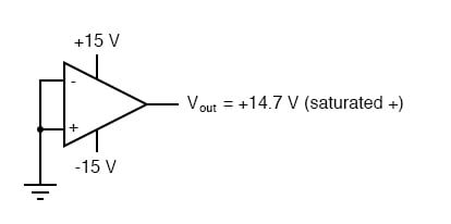
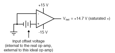
A perfect op-amp would output exactly zero volts with both its inputs shorted together and grounded. However, most op-amps off the shelf will drive their outputs to a saturated level, either negative or positive. In the example shown above, the output voltage is saturated at a value of positive 14.7 volts, just a bit less than +V (+15 volts) due to the positive saturation limit of this particular op-amp. Because the offset in this op-amp is driving the output to a completely saturated point, there’s no way of telling how much voltage offset is present at the output. If the +V/-V split power supply was of a high enough voltage, who knows, maybe the output would be several hundred volts one way or the other due to the effects of offset!
For this reason, offset voltage is usually expressed in terms of the equivalent amount of input voltage differential producing this effect. In other words, we imagine that the op-amp is perfect (no offset whatsoever), and a small voltage is being applied in series with one of the inputs to force the output voltage one way or the other away from zero. Being that op-amp differential gains are so high, the figure for “input offset voltage” doesn’t have to be much to account for what we see with shorted inputs:
Offset voltage will tend to introduce slight errors in any op-amp circuit. So how do we compensate for it? Unlike common-mode gain, there are usually provisions made by the manufacturer to trim the offset of a packaged op-amp. Usually, two extra terminals on the op-amp package are reserved for connecting an external “trim” potentiometer. These connection points are labeled offset null and are used in this general way:
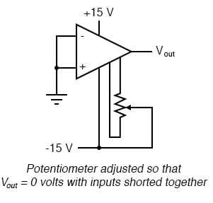
On single op-amps such as the 741 and 3130, the offset null connection points are pins 1 and 5 on the 8-pin DIP package. Other models of op-amp may have the offset null connections located on different pins, and/or require a slightly difference configuration of trim potentiometer connection. Some op-amps don’t provide offset null pins at all! Consult the manufacturer’s specifications for details.
Bias Current
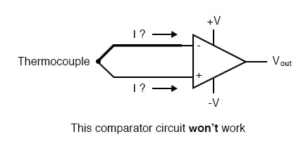
Inputs on an op-amp have extremely high input impedances. That is, the input currents entering or exiting an op-amp’s two input signal connections are extremely small. For most purposes of op-amp circuit analysis, we treat them as though they don’t exist at all. We analyze the circuit as though there was absolutely zero current entering or exiting the input connections. This idyllic picture, however, is not entirely true. Op-amps, especially those op-amps with bipolar transistor inputs, have to have some amount of current through their input connections in order for their internal circuits to be properly biased. These currents, logically, are called bias currents. Under certain conditions, op-amp bias currents may be problematic. The following circuit illustrates one of those problem conditions:
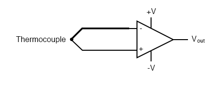
At first glance, we see no apparent problems with this circuit. A thermocouple, generating a small voltage proportional to temperature (actually, a voltage proportional to the difference in temperature between the measurement junction and the “reference” junction formed when the alloy thermocouple wires connect with the copper wires leading to the op-amp) drives the op-amp either positive or negative. In other words, this is a kind of comparator circuit, comparing the temperature between the end thermocouple junction and the reference junction (near the op-amp). The problem is this: the wire loop formed by the thermocouple does not provide a path for both input bias currents, because both bias currents are trying to go the same way (either into the op-amp or out of it).
In order for this circuit to work properly, we must ground one of the input wires, thus providing a path to (or from) ground for both currents:
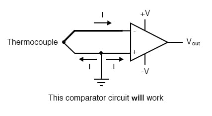
Not necessarily an obvious problem, but a very real one!
Another way input bias currents may cause trouble is by dropping unwanted voltages across circuit resistances. Take this circuit for example:
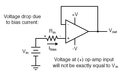
We expect a voltage follower circuit such as the one above to reproduce the input voltage precisely at the output. But what about the resistance in series with the input voltage source? If there is any bias current through the noninverting (+) input at all, it will drop some voltage across Rin, thus making the voltage at the noninverting input unequal to the actual Vin value. Bias currents are usually in the microamp range, so the voltage drop across Rin won’t be very much, unless Rin is very large. One example of an application where the input resistance (Rin) would be very large is that of pH probe electrodes, where one electrode contains an ion-permeable glass barrier (a very poor conductor, with millions of Ω of resistance).
If we were actually building an op-amp circuit for pH electrode voltage measurement, we’d probably want to use a FET or MOSFET (IGFET) input op-amp instead of one built with bipolar transistors (for less input bias current). But even then, what slight bias currents may remain can cause measurement errors to occur, so we have to find some way to mitigate them through good design.
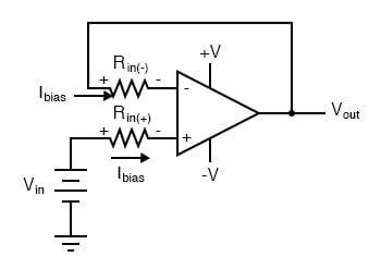
One way to do so is based on the assumption that the two input bias currents will be the same. In reality, they are often close to being the same, the difference between them referred to as the input offset current. If they are the same, then we should be able to cancel out the effects of input resistance voltage drop by inserting an equal amount of resistance in series with the other input, like this:
With the additional resistance added to the circuit, the output voltage will be closer to Vin than before, even if there is some offset between the two input currents.
For both inverting and noninverting amplifier circuits, the bias current compensating resistor is placed in series with the noninverting (+) input to compensate for bias current voltage drops in the divider network:
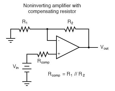
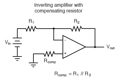
In either case, the compensating resistor value is determined by calculating the parallel resistance value of R1 and R2. Why is the value equal to the parallel equivalent of R1 and R2? When using the Superposition Theorem to figure how much voltage drop will be produced by the inverting (-) input’s bias current, we treat the bias current as though it were coming from a current source inside the op-amp and short-circuit all voltage sources (Vin and Vout). This gives two parallel paths for bias current (through R1 and through R2, both to ground). We want to duplicate the bias current’s effect on the noninverting (+) input, so the resistor value we choose to insert in series with that input needs to be equal to R1 in parallel with R2.
A related problem, occasionally experienced by students just learning to build operational amplifier circuits, is caused by a lack of a common ground connection to the power supply. It is imperative to proper op-amp function that some terminal of the DC power supply be common to the “ground” connection of the input signal(s). This provides a complete path for the bias currents, feedback current(s), and for the load (output) current. Take this circuit illustration, for instance, showing a properly grounded power supply:
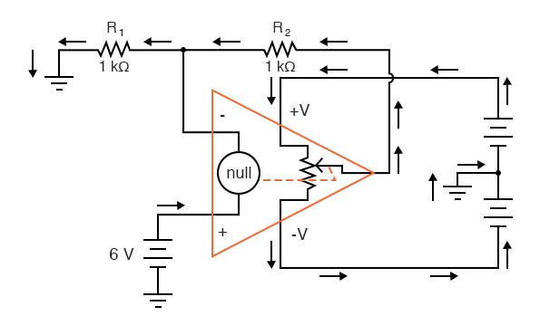
Here, arrows denote the path of electron flow through the power supply batteries, both for powering the op-amp’s internal circuitry (the “potentiometer” inside of it that controls output voltage), and for powering the feedback loop of resistors R1 and R2. Suppose, however, that the ground connection for this “split” DC power supply were to be removed. The effect of doing this is profound:
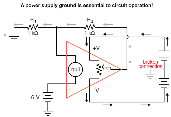
No electrons may flow in or out of the op-amp’s output terminal, because the pathway to the power supply is a “dead end.” Thus, no electrons flow through the ground connection to the left of R1, neither through the feedback loop. This effectively renders the op-amp useless: it can neither sustain current through the feedback loop, nor through a grounded load, since there is no connection from any point of the power supply to ground.
The bias currents are also stopped, because they rely on a path to the power supply and back to the input source through ground. The following diagram shows the bias currents (only), as they go through the input terminals of the op-amp, through the base terminals of the input transistors, and eventually through the power supply terminal(s) and back to ground.
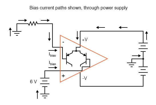
Without a ground reference on the power supply, the bias currents will have no complete path for a circuit, and they will halt. Since bipolar junction transistors are current-controlled devices, this renders the input stage of the op-amp useless as well, as both input transistors will be forced into cutoff by the complete lack of base current.
REVIEW:
- Op-amp inputs usually conduct very small currents, called bias currents, needed to properly bias the first transistor amplifier stage internal to the op-amps’ circuitry. Bias currents are small (in the microamp range), but large enough to cause problems in some applications.
- Bias currents in both inputs must have paths to flow to either one of the power supply “rails” or to ground. It is not enough to just have a conductive path from one input to the other.
- To cancel any offset voltages caused by bias current flowing through resistances, just add an equivalent resistance in series with the other op-amp input (called a compensating resistor). This corrective measure is based on the assumption that the two input bias currents will be equal.
- Any inequality between bias currents in an op-amp constitutes what is called an input offset current.
- It is essential for proper op-amp operation that there be a ground reference on some terminal of the power supply, to form complete paths for bias currents, feedback current(s), and load current.
Drift
Being semiconductor devices, op-amps are subject to slight changes in behavior with changes in operating temperature. Any changes in op-amp performance with temperature fall under the category of op-amp drift. Drift parameters can be specified for bias currents, offset voltage, and the like. Consult the manufacturer’s data sheet for specifics on any particular op-amp.
To minimize op-amp drift, we can select an op-amp made to have minimum drift, and/or we can do our best to keep the operating temperature as stable as possible. The latter action may involve providing some form of temperature control for the inside of the equipment housing the op-amp(s). This is not as strange as it may first seem. Laboratory-standard precision voltage reference generators, for example, are sometimes known to employ “ovens” for keeping their sensitive components (such as zener diodes) at constant temperatures. If extremely high accuracy is desired over the usual factors of cost and flexibility, this may be an option worth looking at.
REVIEW:
- Op-amps, being semiconductor devices, are susceptible to variations in temperature. Any variations in amplifier performance resulting from changes in temperature is known as drift. Drift is best minimized with environmental temperature control.
Frequency Response
With their incredibly high differential voltage gains, op-amps are prime candidates for a phenomenon known as feedback oscillation. You’ve probably heard the equivalent audio effect when the volume (gain) on a public-address or other microphone amplifier system is turned too high: that high pitched squeal resulting from the sound waveform “feeding back” through the microphone to be amplified again. An op-amp circuit can manifest this same effect, with the feedback happening electrically rather than audibly.
A case example of this is seen in the 3130 op-amp, if it is connected as a voltage follower with the bare minimum of wiring connections (the two inputs, output, and the power supply connections). The output of this op-amp will self-oscillate due to its high gain, no matter what the input voltage. To combat this, a small compensation capacitor must be connected to two specially-provided terminals on the op-amp. The capacitor provides a high-impedance path for negative feedback to occur within the op-amp’s circuitry, thus decreasing the AC gain and inhibiting unwanted oscillations. If the op-amp is being used to amplify high-frequency signals, this compensation capacitor may not be needed, but it is absolutely essential for DC or low-frequency AC signal operation.
Some op-amps, such as the model 741, have a compensation capacitor built in to minimize the need for external components. This improved simplicity is not without a cost: due to that capacitor’s presence inside the op-amp, the negative feedback tends to get stronger as the operating frequency increases (that capacitor’s reactance decreases with higher frequencies). As a result, the op-amp’s differential voltage gain decreases as frequency goes up: it becomes a less effective amplifier at higher frequencies.
Op-amp manufacturers will publish the frequency response curves for their products. Since a sufficiently high differential gain is absolutely essential to good feedback operation in op-amp circuits, the gain/frequency response of an op-amp effectively limits its “bandwidth” of operation. The circuit designer must take this into account if good performance is to be maintained over the required range of signal frequencies.
REVIEW:
- Due to capacitances within op-amps, their differential voltage gain tends to decrease as the input frequency increases. Frequency response curves for op-amps are available from the manufacturer.
Input to Output Phase Shift
In order to illustrate the phase shift from input to output of an operational amplifier (op-amp), the OPA227 was tested in our lab. The OPA227 was constructed in a typical non-inverting configuration (Figure below).
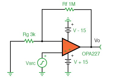
OPA227 Non-inverting stage
The circuit configuration calls for a signal gain of ≅34 V/V or ≅50 dB. The input excitation at Vsrc was set to 10 mVp, and three frequencies of interest: 2.2 kHz, 22 kHz, and 220 MHz. The OPA227’s open loop gain and phase curve vs. frequency is shown in Figure below.
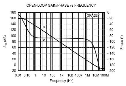
AV and Φ vs. Frequency plot
To help predict the closed loop phase shift from input to output, we can use the open loop gain and phase curve. Since the circuit configuration calls for a closed loop gain, or 1/β, of ≅50 dB, the closed loop gain curve intersects the open loop gain curve at approximately 22 kHz. After this intersection, the closed loop gain curve rolls off at the typical 20 dB/decade for voltage feedback amplifiers, and follows the open loop gain curve.
What is actually at work here is the negative feedback from the closed loop modifies the open loop response. Closing the loop with negative feedback establishes a closed loop pole at 22 kHz. Much like the dominant pole in the open loop phase curve, we will expect phase shift in the closed loop response. How much phase shift will we see?
Since the new pole is now at 22 kHz, this is also the -3 dB point as the pole starts to roll off the closed loop again at 20 dB per decade as stated earlier. As with any pole in basic control theory, phase shift starts to occur one decade in frequency before the pole, and ends at 90o of phase shift one decade in frequency after the pole. So what does this predict for the closed loop response in our circuit?
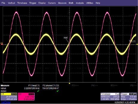
This will predict phase shift starting at 2.2 kHz, with 45o of phase shift at the -3 dB point of 22 kHz, and finally ending with 90o of phase shift at 220 kHz. The three Figures shown below are oscilloscope captures at the frequencies of interest for our OPA227 circuit. Figure below is set for 2.2 kHz, and no noticeable phase shift is present. Figure below is set for 220 kHz, and ≅45o of phase shift is recorded. Finally, Figure below is set for 220 MHz, and the expected ≅90o of phase shift is recorded. The scope plots were captured using a LeCroy 44x Wavesurfer. The final scope plot used a x1 probe with the trigger set to HF reject.
OPA227 Av=50dB @ 2.2 kHz
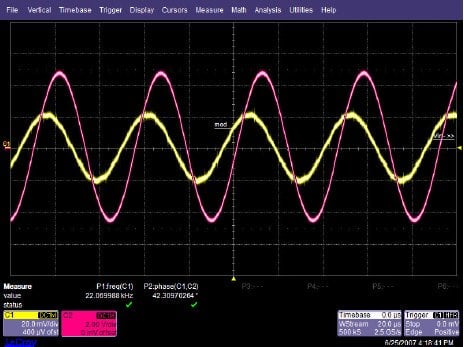
OPA227 Av=50dB @ 22 kHz
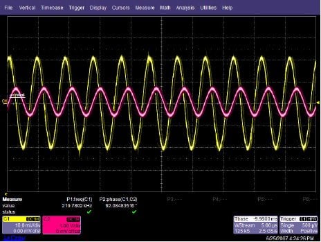
OPA227 Av=50dB @ 220 kHz
RELATED WORKSHEETS:
- Summer and Subtractor OpAmp Circuits Worksheet
-
Inverting and Noninverting OpAmp Voltage Amplifier Circuits Worksheet


Thanks a lot for this textbook! Is it possible that there’s a typo concerning the signal gain? Looking at the circuit I get ~334V/V instead of the mentioned 34V/V. (334V/V would be consistent with the result of ~50dB)