Facebook
 Google
 GitHub
 Linkedin
Building a Differential Amplifier
Differential Op-Amp Circuits
An op-amp with no feedback is already a differential amplifier, amplifying the voltage difference between the two inputs. However, its gain cannot be controlled, and it is generally too high to be of any practical use. So far, our application of negative feedback to op-amps has resulting in the practical loss of one of the inputs, the resulting amplifier only good for amplifying a single voltage signal input. With a little ingenuity, however, we can construct an op-amp circuit maintaining both voltage inputs, yet with a controlled gain set by external resistors.
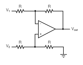
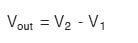
If all the resistor values are equal, this amplifier will have a differential voltage gain of 1. The analysis of this circuit is essentially the same as that of an inverting amplifier, except that the noninverting input (+) of the op-amp is at a voltage equal to a fraction of V2, rather than being connected directly to ground. As would stand to reason, V2 functions as the noninverting input and V1 functions as the inverting input of the final amplifier circuit. Therefore:
If we wanted to provide a differential gain of anything other than 1, we would have to adjust the resistances in both upper and lower voltage dividers, necessitating multiple resistor changes and balancing between the two dividers for symmetrical operation. This is not always practical, for obvious reasons.
Buffer the Input Voltage Signal
Another limitation of this amplifier design is the fact that its input impedances are rather low compared to that of some other op-amp configurations, most notably the noninverting (single-ended input) amplifier. Each input voltage source has to drive current through a resistance, which constitutes far less impedance than the bare input of an op-amp alone. The solution to this problem, fortunately, is quite simple. All we need to do is “buffer” each input voltage signal through a voltage follower like this:
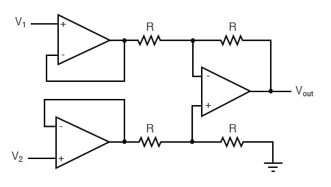
Now the V1 and V2 input lines are connected straight to the inputs of two voltage-follower op-amps, giving very high impedance. The two op-amps on the left now handle the driving of current through the resistors instead of letting the input voltage sources (whatever they may be) do it. The increased complexity to our circuit is minimal for a substantial benefit.
RELATED WORKSHEETS: