 Facebook
 Google
 GitHub
 Linkedin
The Basic MOSFET Constant-Current Source
Learn about a straightforward version of a circuit that is essential in the design of analog integrated circuits.
Learn about a straightforward version of a circuit that is essential in the design of analog integrated circuits.
Supporting Information
- Bipolar Junction Transistors: Current Mirrors
- Discrete Semiconductor Circuits: Current Mirror
- Insulated-Gate Field-Effect Transistors (MOSFET)
What Is the Elusive Current Source?
Constant-current sources figure prominently in circuit-analysis exercises and network theorems, then they seem to more or less disappear . . . unless you’re an IC designer. Though rarely encountered in typical PCB design, current sources are ubiquitous in the world of analog ICs. This is because they are used 1) for biasing and 2) as active loads.
- Biasing: Transistors functioning as linear amplifiers need to be biased such that they are operating in a desirable portion of their transfer characteristic. The best way to do this in the context of IC design is to cause a predetermined current to flow through the transistor’s drain (for MOSFETs) or collector (for BJTs). This predetermined current needs to be stable and independent of the voltage across the current-source component. Of course, no real circuit will ever be perfectly stable or perfectly immune to changes in voltage, but as is usually the case in engineering, perfection is not quite necessary.
- Active loads: In amplifier circuits, current sources can be used instead of collector/drain resistors. These “active loads” provide higher voltage gain and allow the circuit to function properly with lower supply voltage. Also, IC manufacturing technology favors transistors over resistors.
Throughout this article, I’ll refer to the output of the current source as “bias current” or IBIAS, because I think that the biasing application is a more straightforward vehicle for pondering this circuit’s basic functionality.
The MOSFET Constant-Current Source Circuit
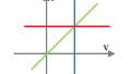
Here is the basic MOSFET constant-current source:
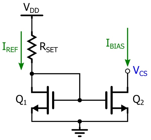
It’s surprisingly simple, in my opinion—two NMOS transistors and a resistor. Let’s look at how this circuit works.
As you can see, the drain of Q1 is shorted to its gate. This means that VG = VD, and thus VGD = 0 V. So, is Q1 in cutoff, the triode region, or the saturation region? It can’t be in cutoff, because if no current were flowing through the channel, the gate voltage would be at VDD, and thus VGS would be greater than the threshold voltage VTH (we can safely assume that VDD is higher than VTH). This means Q1 will always be in saturation (also referred to as “active” mode), because VGD = 0 V, and one way of expressing the condition for MOSFET saturation is that VGD must be less than VTH.
If we recall that no steady-state current flows into the gate of a MOSFET, we can see that the reference current IREF will be the same as Q1’s drain current. We can customize this reference current by choosing an appropriate value for RSET. So what does all this have to do with Q2? Well, the drain current of a MOSFET in saturation is influenced by the width-to-length ratio of the channel and the gate-to-source voltage:
\[I_D=\frac{1}{2}\mu_nC_{ox}\frac{W}{L}(V_{GS}-V_{TH})^2\]
At this point we are ignoring channel-length modulation; consequently, as indicated by the equation, the drain current is not affected by the drain-to-source voltage. Now notice that both FETs have their sources tied to ground and that their gates are shorted together—in other words, both have the same gate-to-source voltage. Thus, if we assume that both devices have the same channel dimensions, their drain currents will be equal, regardless of the voltage at the drain of Q2. This voltage is labeled VCS, meaning the voltage across the current-source component; this helps to remind us that Q2, like any well-behaved current source, generates a bias current that is not affected by the voltage across its terminals. Another way to say this is that Q2 has infinite output resistance:
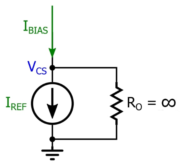
Under these conditions, no current ever flows through the output resistance RO, even when VCS is very high. This means that the bias current is always exactly equal to the reference current.
A common name for this circuit is a “current mirror.” You can probably see why—the current generated by the right-hand transistor mirrors (i.e., is similar to) the reference current flowing through the left-hand transistor. And the name is particularly appropriate when you consider the visual symmetry exhibited by the typical schematic representation.
By the way, older ICs often required an external resistor for RSET. Nowadays, though, manufacturers use on-chip resistors that have been trimmed in order to achieve adequate precision.
The Importance of the Transistor Staying in Saturation
The first major affront to the idealized analysis of this circuit is the fact that everything falls apart when the transistor is not in saturation. If Q2 is in the triode (AKA linear) region, the drain current will be highly dependent on VDS. In other words, we no longer have a current source because the bias current is affected by VCS. We know that Q2’s gate-to-drain voltage must be less than the threshold voltage to maintain saturation.
Another way to say this is that Q2 will leave the saturation region when the drain voltage becomes VTH volts lower than the gate voltage. We can’t put a precise number on this because both the gate voltage and the threshold voltage will vary from one implementation to another.
A reasonable example is the following: The gate voltage required to generate the desired bias current is around 0.9 V, and the threshold voltage is 0.6 V; this means we can maintain saturation as long as VCS stays above ~0.3 V.
Channel-Length Modulation
Unfortunately, even when our overall circuit design ensures that Q2 will always be in saturation, our MOSFET current source is not exactly ideal. The culprit is channel-length modulation.
The essence of the saturation region is the “pinched-off” channel that exists when the gate-to-drain voltage does not exceed the threshold voltage.
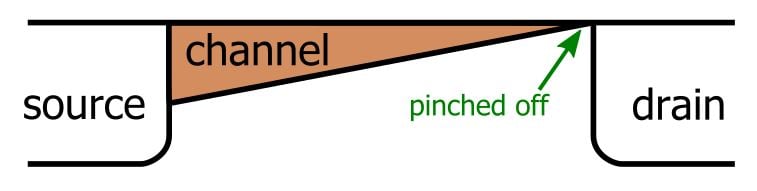
The idea is that drain current becomes independent of VDS after the channel is pinched off because further increases in drain voltage do not affect the shape of the channel. In reality, though, increases in VDS cause the “pinch-off point” to move toward the source, and this allows the drain voltage to have a small effect on the drain current even when the FET is in saturation. The result can be represented as follows:
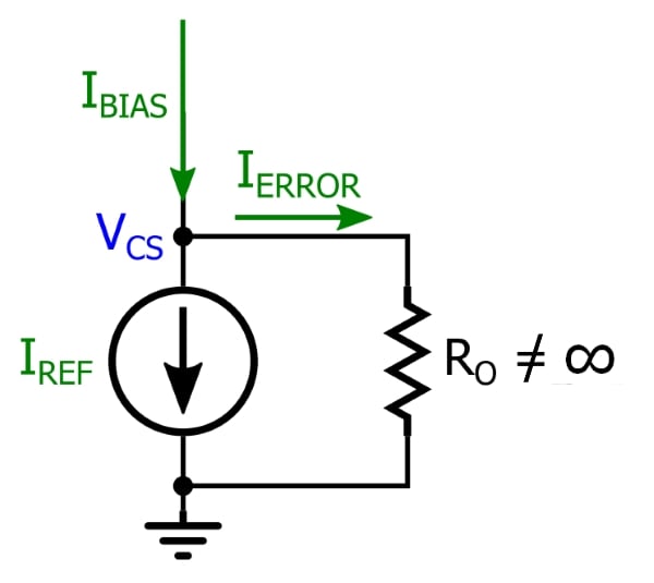
IBIAS is now the sum of IREF (determined by RSET) and IERROR (the current flowing through the output resistance). IERROR obeys the simple Ohm’s law relationship: higher VCS means more IERROR and consequently more IBIAS, and thus the current source is no longer independent of the voltage across its terminals.
Adjusting and Steering
This handy current-source circuit becomes even better when you realize how flexible it is. First let’s look at adjusting the current generated by Q2. So far we’ve assumed that the generated current is the same as the reference current, but this is true only when the transistors have the same channel-width-to-channel-length ratio. Remember the equation for saturation-mode drain current:
\[I_D=\frac{1}{2}\mu_nC_{ox}\frac{W}{L}(V_{GS}-V_{TH})^2\]
Drain current is directly proportional to the width-to-length ratio, and thus we can increase or decrease IBIAS simply by making Q2’s W/L ratio higher than or lower than that of Q1. For example, if we want the bias current to be two times larger than the reference current, all we need to do is keep the channel lengths the same and increase Q2’s channel width by a factor of two. (This may not seem so easy if you’re used to working with discrete FETs, but specifying channel dimensions is standard practice in IC design.)
It is also quite straightforward to use this circuit for “current steering.” The following diagram illustrates the current-steering concept:
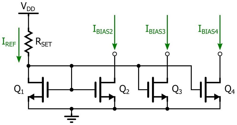
This clever arrangement allows us to generate multiple bias currents from one reference current. Even better, each of these currents can be different—they can be individually modified simply by adjusting the width-to-length ratios.
Conclusion
We’ve covered the operation and capabilities of the basic MOSFET constant-current source, and we also discussed limitations. As implied by the adjective “basic,” there are better circuits out there. But the basic circuit is a good place to start, because the two-transistor current mirror remains the conceptual core of the higher-performance topologies.
Related Content


Hi,
Apart from trial and error, is there any way to calculate the Iref? Some datasheets do not provide all info needed on you formulas
TIA
If the load goes from Vcs to GND, what is supplying the voltage for I-bias? There’s not anything being “supplied” with the constant current in these diagrams. If it goes where the I-bias is, then what’s above that?