Facebook
 Google
 GitHub
 Linkedin
How SoC Integration Impacts SMT Assembly Yield
Learn how SoC integration impacts SMT assembly yield, from fine-pitch BGA challenges and package warpage to reflow profiling and inspection strategies.
The System-on-Chip (SoC) is contradictory; it simplifies the schematics, but complicates the assembly. The embedding of an entire computer, consisting of a CPU, GPU, and memory, into one die decreases the number of components but significantly increases the difficulty in solder joint connections.
Moving from standard 0.8mm pitch components to 0.35mm pitch SoCs collapses the manufacturing process window. In this high-density environment, First Pass Yield (FPY) isn't just a metric - it's the difference between profit and scrap. A single failed BGA joint renders the entire assembly defective, and reworking high-value silicon risks latent defects.
To scale successfully, SMT assembly must be treated as a precision-engineered physics problem.
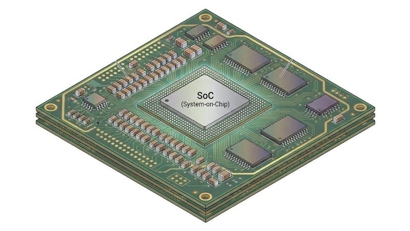
Figure 1. Illustration of a System-on-Chip (SoC) mounted on a PCBA, highlighting the high-density SMT assembly environment.
Why SoCs are Difficult to Solder?
SoCs introduce three primary adversarial forces: reduced process windows, aperture limits, and dynamic warpage.
Fine-Pitch Process Window Reduction
- 0.8 mm Pitch: A standard BGA ball (~0.5mm) self-corrects minor placement offsets during reflow due to surface tension.
- 0.35 mm Pitch: The ball diameter shrinks to approximately 0.2 mm. A 0.05 mm placement error or a 10% reduction in paste volume can result in an "open" joint. The process window effectively collapses, requiring tighter machine control.
- Gasketing Efficiency: At this pitch, the solder mask web between pads is often <0.1 mm. If the stencil does not form a perfect seal (gasket) against the mask, paste will bleed underneath the stencil bridge, creating invisible shorts that only appear after reflow.
Stencil Aperture Aspect Ratio Limits
The solder paste stencil is critical for yield. The IPC-7525 standard dictates that the Area Ratio (AR)---the area of the aperture opening divided by the area of the aperture walls—must exceed 0.66.
If the AR drops below 0.66, friction causes paste to clog the stencil rather than depositing on the board. For a 0.35 mm pitch SoC with a 0.2 mm aperture, a standard 0.1mm stencil yields an AR of 0.5. Without electropolishing or nano-coating, this guarantees insufficient solder volume, leading to "open" joints or weak intermetallic bonds.
Dynamic Package Warpage During Reflow
The most insidious threat is the Coefficient of Thermal Expansion (CTE) Mismatch. The silicon die, organic substrate, and FR-4 PCB expand at different rates.
During the time that the assembly is passing through the reflow oven, the SoC package adjusts its shape in a dynamic manner.
- Transition Zone (150°C - 190°C): The organic substrate is growing at a rate quicker than that of the silicon die, which is resulting in the corners being curled downward ("Frown").
- Peak Zone (>217°C): The warpage may invert or relax. If the corners lift by tens of microns (often exceeding package or JEDEC-defined limits) while the solder is molten, the ball separates from the paste. Upon cooling, it drops back down on frozen flux, failing to form a bond.
Critical Defect Mechanisms in SoC SMT Assembly
Head-in-Pillow (HiP)
Head-in-Pillow is one of the most characteristic defects of SoC assembly. It occurs when the BGA sphere and solder paste melt individually but fail to coalesce.
Mechanism: Warpage lifts the ball off the paste during the soak zone. The exposed surfaces oxidize rapidly. When the package settles, the oxidation layer prevents mixing, creating a contact that passes DC electrical testing but fails under mechanical stress.
Non-Wet Open (NWO)
Non-Wet Open occurs when the solder paste flux is exhausted before reflow. If the thermal profile keeps the board in the "Soak Zone" too long, volatiles evaporate. At peak temperature, no active flux remains to remove oxides, causing the solder ball to retract.
Solder Bridging
Bridging is rarely caused by placement inaccuracy in fine-pitch SoCs. Instead, it stems from Paste Slump (viscosity dropping during heating) or poor gasketing between the stencil and PCB.
Voiding
While IPC standards allow 25% voiding, excessive voiding in SoCs weakens joints. The primary culprit in HDI designs is Via-in-Pad outgassing. During reflow, if the VIA are not properly plated over (POFV), maximum entrapped air expands to cause air entrapped on the top side of the board to blow into the molten joint.
| Defect Type | Root Cause (Physics) | Primary Process Mitigation |
| Head-in-Pillow (HiP) | Warpage / Oxidation | Optimized Profile, Nitrogen (N₂) Reflow |
| Solder Bridging | Excess Paste / Gasketing | Step-Down Stencil, Nano-Coating |
| Non-Wet Open (NWO) | Flux Exhaustion | Reduced Soak Time, Active Flux |
| Voiding | Outgassing | Via Capping (POFV), Vacuum Reflow |
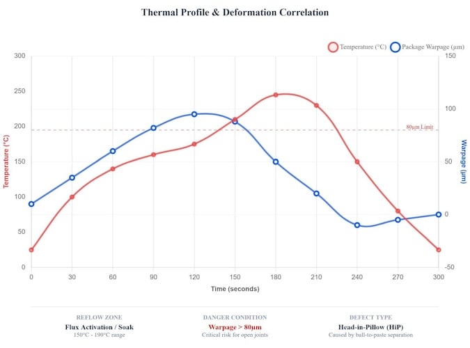
Figure 2. Graph correlating SoC package dynamic warpage with reflow temperature zones, identifying the risk window for Head-in-Pillow defects.
Process Control: Engineering for High SMT Yield
Stencil Technology
Standard laser-cut stencils are insufficient for SoCs.
- Nano-Coatings: A hydrophobic coating reduces surface energy, allowing paste to release cleanly even at low area ratios (0.55).
- Step-Down Stencils: Selective thinning of the stencil foil in the SoC area (for example, 0.12mm to 0.10mm) guarantees the right volume for fine-pitch pads without creating a shortage for larger components.
Reflow Profiling Strategies
- Soak Zone Optimization: Switching to a "Ramp-to-Spike" (RTS) profile minimizes the time flux is exposed to heat before reflow, preserving activity.
- Nitrogen (N₂) Atmosphere: Performing the reflow process in a Nitrogen atmosphere (<1,000 PPM Oxygen) allows for the lowering of solder surface tension and, at the same time, the prevention of re-oxidation during warpage events, leading to a drastic reduction in HiP defects.
Solder Paste Selection
Type 5 paste (15–25µm particle size) is required for <0.4mm pitch SoCs. The smaller spheres pack tighter into miniature apertures than standard Type 4, improving print definition.
Inspection Blind Spots: You Cannot Fix What You Cannot See
Automated Optical Inspection (AOI) is not able to check BGA bonds that are concealed by silicon.
Automated X-Ray Inspection (AXI)
- 2D Transmission X-Ray: Good for detecting shorts, but struggles to detect "open" joints like HiP, where the ball and pad overlap vertically.
- 3D Laminography: Takes image slices at different depths, separating the BGA ball from the pad. It can analyze the "slice" at the interface to confirm wetting.
Destructive Analysis (Dye & Pry)
During NPI, Dye & Pry accompany the calibration of the inspection. The red dye is injected under the BGA, vacuumed, and subjected to heat. By taking out the component, any broken or open connections that are stained with red could be detected, which in turn would provide ground-truth validation for the X-ray process.
All images used courtesy of JLCPCB.