Facebook
 Google
 GitHub
 Linkedin
Output Voltage and Diode Current in a Boost Converter
Learn how output voltage and diode current affect the behavior of a step-up switching regulator.
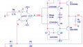
In the preceding articles, we used the LTspice schematic in Figure 1 to explore design decisions and operational details of a basic step-up DC/DC converter. Now we’ll continue our examination of the boost converter topology by analyzing the electrical behavior of its output components.

Figure 1. Schematic of a boost converter implemented in LTspice.
Output Voltage and Ripple
The circuit is currently configured to convert a 2.5 V input voltage into a 5 V output voltage; as we can see in Figure 2, the actual output voltage is 4.94 V. We could make small adjustments to the duty cycle if we wanted to fine-tune the output voltage, but there’s really no need—a real-life implementation would use feedback to ensure that VOUT stays very close to the nominal value despite variations in load current and input voltage.
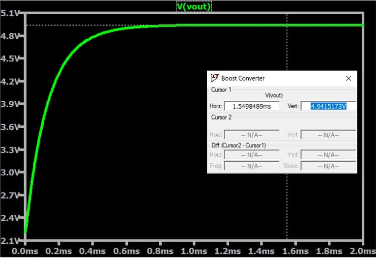
Figure 2. Output voltage for the boost converter in Figure 1.
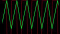
After startup, the output capacitor charges up and the output voltage gradually increases toward its final value. Figure 3 shows startup behavior for four different values of COUT. (COUT is represented by one capacitor, C1, in my schematic; in a physical circuit, COUT will often consist of multiple capacitors.)
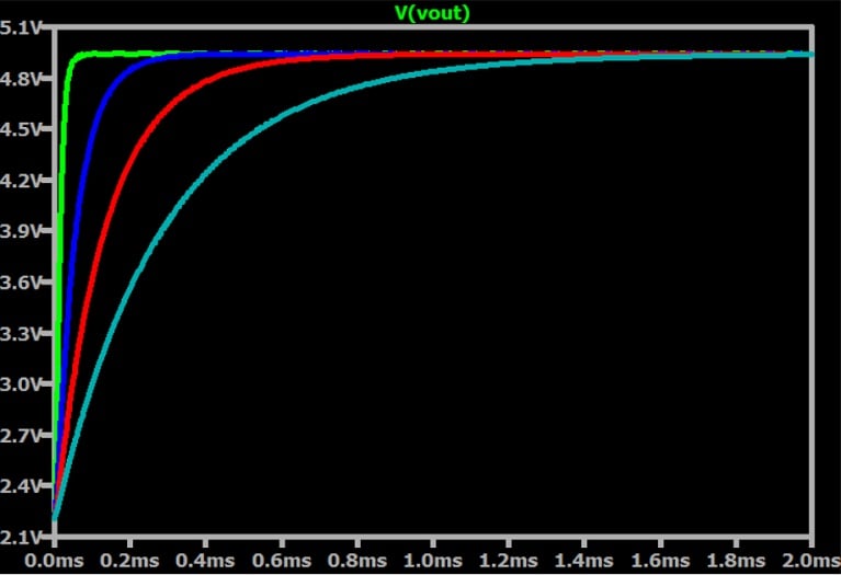
Figure 3. Boost converter startup behavior for four different values of COUT: 5 μF (green trace), 20 μF (blue trace), 47 μF (red trace), and 100 μF (cyan trace).
The output capacitance value affects the amount of time required to reach an acceptable output voltage after startup. If you have an application that requires rapid startup, you might need to reduce COUT by using a smaller capacitor.
Let’s go back to our original COUT of 47 μF and take a look at the ripple (Figure 4).
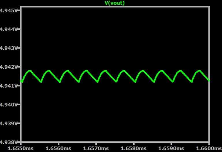
Figure 4. Output ripple for COUT = 47 μF.
Our simulated peak-to-peak ripple is less than 1 mV, which is extremely low. We’ll discuss why in the next section.
Before that, though, we started with a generous amount of output capacitance for a compact, low-power circuit like this one. Figure 5 shows what happens when we reduce COUT to 4.7 μF.
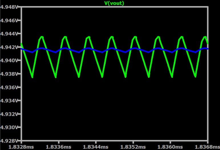
Figure 5. Output ripple for COUT = 4.7 μF (green trace) and COUT = 47 μF (blue trace).
As you can see, ripple increases as output capacitance decreases.
Equivalent Series Resistance
Our simulated circuit lacks the non-idealities we would expect in an actual boost converter, so the output ripple above is unrealistically low. To understand how a boost converter behaves in real life, we need to consider the role of the capacitor’s equivalent series resistance (ESR), which generates ripple voltage independently of the amount of capacitance.
We saw in the preceding article that our small inductance resulted in more inductor current ripple. As this large ΔIL makes its way to the output capacitor, its passage through the capacitor’s ESR creates proportionally large voltage drops. These voltage drops contribute to output ripple.
Figure 6 illustrates the difference in output ripple between 47 μF output capacitance with zero ESR (the green trace) and 47 μF output capacitance with 10 mΩ of ESR (the blue trace).
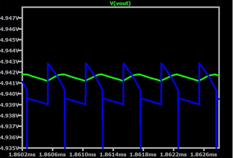
Figure 6. Voltage ripple for two different ESR values. COUT = 47 μF.
The equivalent series inductance of the output capacitor also affects output ripple. It’s a complicated topic which I don’t intend to address in depth today, but I recommend a Texas Instruments app note entitled “Measuring and Understanding the Output Voltage Ripple of a Boost Converter” if you’re interested in learning more.
Diode Current
We have one more output component to discuss today: the diode.
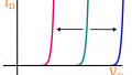
We can see in Figure 7 that the average diode current in a boost converter corresponds to the load current, just like the average inductor current does in a buck converter. That’s not surprising: if we compare the boost and buck component arrangements, we see that the boost has the diode where the buck has the converter.
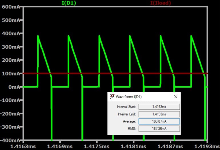
Figure 7. A comparison of average diode current and load current for the boost converter in Figure 1.
Reverse-Recovery Current
If you’re wondering about the negative-going spikes in Figures 6 and 7, they’re caused by the rapid burst of current that flows through the diode and the switch right after the switch closes. You can see this behavior more clearly below, in Figure 8.
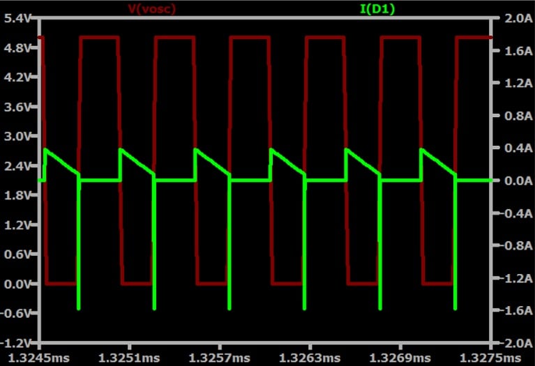
Figure 8. Switching voltage (red trace) and diode current (green trace).
The spike current is reported as negative, which in the context of this simulation indicates that it is reverse (i.e., cathode-to-anode) diode current. This current is associated with the phenomenon called reverse recovery, which occurs when a diode’s forward-bias voltage rapidly transitions to a reverse-bias voltage.
As we saw above, the reverse-recovery current has a major impact on the output voltage if you add ESR to your capacitor; the burst of current flows upward through the output capacitor and gets converted into negative-going spike voltage by the cap’s resistance. Things get much worse if you add equivalent series inductance, which presents a particularly hefty impedance to the very high frequencies contained in a sharp spike like that one.
If you want to eliminate this spike behavior from your simulations, you can use an idealized diode instead of one of the diodes that has a realistic SPICE model.
Wrapping Up
This article concludes my series on boost converters—I hope it has helped you gain a more thorough understanding of this important circuit topology. In my next series of articles, we’ll continue our LTspice journey through switch-mode regulation with the buck-boost converter.
All images used courtesy of Robert Keim
Related Content