 Facebook
 Google
 GitHub
 Linkedin
Inductor Current in a Boost Converter: a SPICE Analysis
With the help of LTspice, we examine how inductor current affects the functioning of a boost converter.
Previous articles in this series covered the design and basic operation of a step-up switching regulator. In this article, we’ll use an LTspice simulation of the circuit in Figure 1 to explore inductor current, output current, and energy transfer.
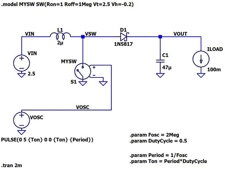
Figure 1. Schematic for a boost converter implemented in LTspice.
Inductor Current Ripple
Figure 2 shows the inductor current of our boost converter in relation to the signal that controls the switch.
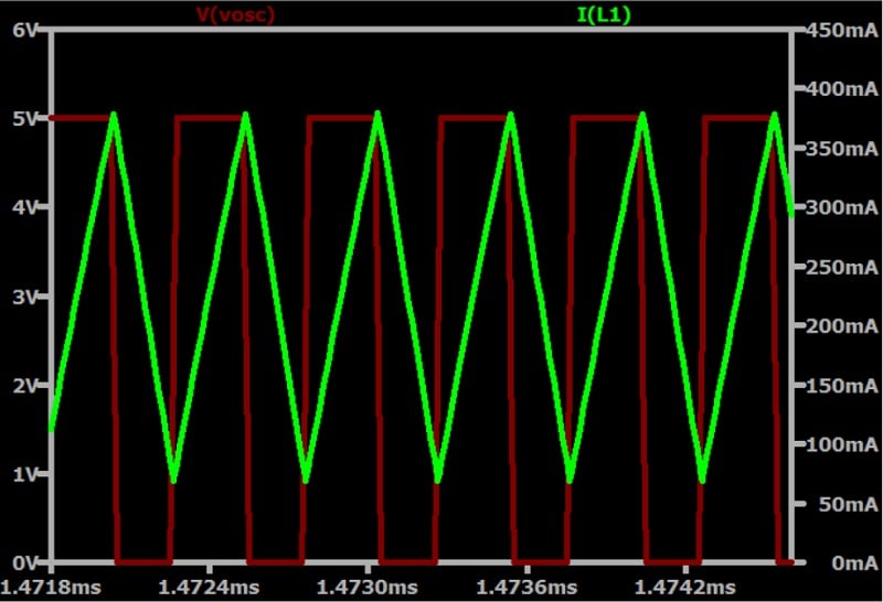
Figure 2. Inductor current (green) in relation to switching voltage (red) for the boost converter in Figure 1.
As expected, the inductor current increases during the switch-on portion of the cycle and decreases during the switch-off portion.
We can also think of this in terms of the inductor charging and discharging:
- When the switch is on, the inductor absorbs energy from the input supply.
- When the switch is off, this energy is transferred to the output capacitor.
In a previous article on switching regulators, I mentioned a rule of thumb according to which the inductor current-ripple magnitude (ΔIL) should be 30% of the maximum load current. In the plot above, though, the current-ripple magnitude is about 300 mA—ten times higher than the 30% value I recommended.
Mathematically, this makes sense. When I created the parameters of this circuit, I initially attempted to generate an inductance value by using a formula; the result was an order of magnitude higher than the 2μH value I ultimately ended up using, and which I chose based on desired component size.
Below is the formula I used:
$$L~=~\frac{V_{IN}~\times~(V_{OUT}~+~V_{D}~–~V_{IN})}{\Delta I_{L(P~–~P)}~\times~f_{SW}~\times~(V_{OUT}~+~V_{D})}$$
All the terms in this equation are defined in the Texas Instruments application note where I originally found it. What’s important for our purposes, though, is that inductance (L) is inversely proportional to ΔIL—so when I decreased the inductance by an order of magnitude, current ripple increased in the same proportion.
Should we be worried about this large ΔIL? It’s not inherently problematic, but I think some concern is justified—particularly if we want to reduce board space and component cost with a small inductor. If that’s the case, we need to consider the following issues during the design process:
- Higher current ripple leads to higher peak currents and generates more EMI.
- The peak inductor current must be lower than the inductor’s saturation current and the maximum allowable switch current.
- With higher current ripple, the converter is more likely to experience discontinuous conduction as load current decreases.
Inductor Current vs. Load Current
Unlike a buck converter, a boost converter’s load current does not equal the average value of its inductor current: instead, the average inductor current is higher. We can see this relationship in Figure 3, which plots the inductor current and load current for the boost converter in Figure 1.
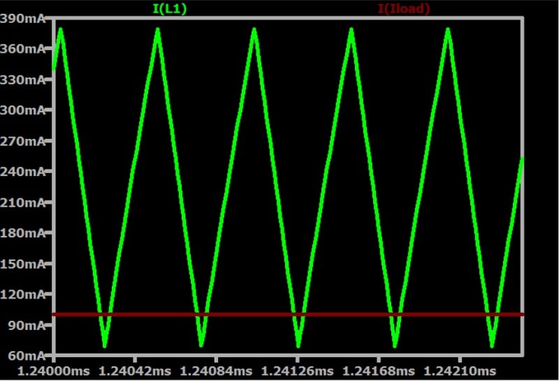
Figure 3. Inductor current (green) in relation to load current (red) for the boost converter in Figure 1.
The voltage on the inductor side of the circuit is lower than the voltage on the output side: to maintain balance, the current on the inductor side is higher on average than the current on the output side. Furthermore, as we see in Figure 4, the magnitude of the voltage across the inductor itself is never as high as the voltage across the load circuitry. The current through the inductor is therefore higher.
Figure 4. Voltage across the inductor (green) versus voltage across the load circuitry (red) for the boost converter in Figure 1.
Energy Transfer
We can make this line of reasoning more mathematically robust by considering energy instead of voltage and current. Figure 5 shows the voltage across the inductor multiplied by the current through the inductor. The inductor’s series resistance is set to zero, meaning that no energy is dissipated by the inductor; the trace thus conveys the quantity of energy that the inductor is storing and releasing.
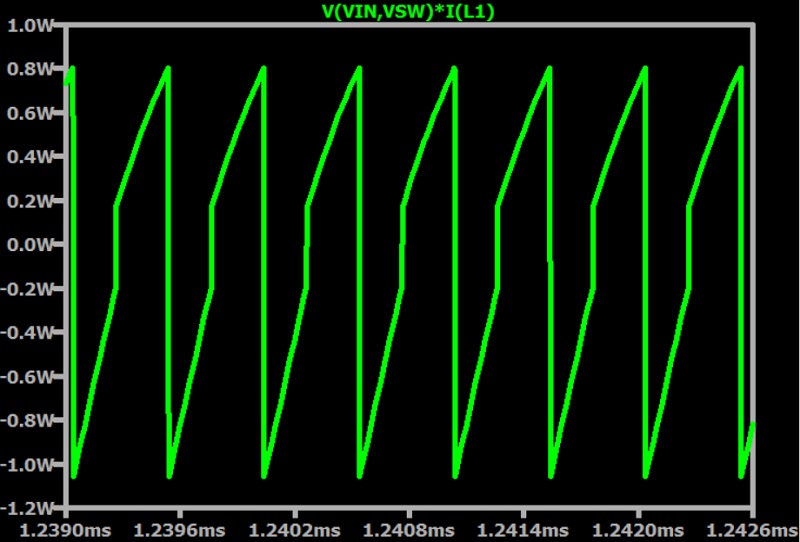
Figure 5. Energy storage over time for the boost converter’s inductor.
TIP: LTspice will automatically generate a power plot like this if you hold down the ALT key while clicking on the relevant component.
Now we’ll use LTspice to display absolute value so that the positive and negative energy don’t cancel each other out (Figure 6).
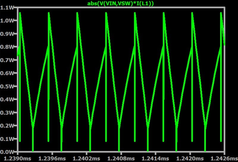
Figure 6. Absolute value of energy storage over time for the boost converter’s inductor.
Next, we want to evaluate the average value of the energy flowing through the inductor (Figure 7).
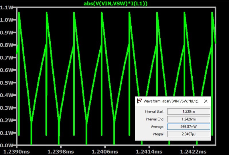
Figure 7. Average energy of the boost converter’s inductor.
TIP: LTspice will calculate the average value of the trace if you hold down the CTRL key while clicking on the trace expression at the top of the graph.
From this, we can see that the energy flow through the inductor is similar to the power delivered to the load. Let’s go through the math:
(VOUT × ILOAD) = (4.94 V × 100 mA) = 494 mW
According to LTspice, the average power dissipated by the switch is 38 mW and the average power dissipated by the diode is 34 mW. If we add these values to the load power, we get the following:
494 mW + 38 mW + 34 mW = 566 mW
The ~70 mW discrepancy occurs because some power is lost as the inductor current flows through the switch (during the charging phase) and through the diode (during the discharging phase).
What’s Next
Understanding the details of inductor current, especially current-ripple magnitude, can help reduce the confusion that often creeps into the SMPS design process. We’ll look at more current and voltage waveforms in the next article—until then, I hope that this article has shed some light on how the inductor current in a boost converter relates to other aspects of the circuit’s electrical behavior.
All images used courtesy of Robert Keim


Could you please explain rule of thumb and why the ripple current should be 30%. I read previous article also. Nothing mentioned about rule of thumb?