Facebook
 Google
 GitHub
 Linkedin
Understanding the Hogge Detector and the Triwave Solution
The Hogge phase detector plays multiple roles in CDR circuits. In this article, we'll explore the Hogge detector's behavior, highlight its main drawbacks, and introduce a different configuration that addresses them.
PLLs are crucial for clock and data recovery (CDR) in asynchronous communication systems, where data is transmitted without a clock signal. In CDR applications, the PLL analyzes random input data to generate a consistent clock signal. Only specific types of phase detectors are suitable for use in these PLLs. One of these is the Hogge detector, which we discussed in the previous article.
The Hogge detector actually plays two key roles in CDR circuits. First, as we just mentioned, it serves as a phase detector. In this capacity, it identifies timing differences between the incoming data and the recovered clock.
Its second role is retiming the data through D flip-flops. These flip-flops, driven by the recovered clock, sample the data at the midpoint of each bit. This process regenerates a cleaner data waveform with lower jitter, ensuring accurate timing for downstream digital logic.
In this article, we'll gain a better understanding of the Hogge detector by examining its input-output characteristic and its limitations. We'll also discuss the triwave phase detector, which addresses the greatest of these limitations.
Input-Output Characteristic of the Hogge Detector
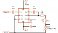
Shown in Figure 1 is the circuit schematic of the Hogge phase detector.

Figure 1. The Hogge phase detector.
The waveforms in Figure 2 illustrate the behavior of the Hogge detector when there is a phase difference between the data and clock signals.
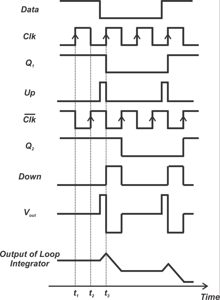
Figure 2. [click to enlarge] Waveforms illustrating the operation of the Hogge detector.
In this scenario, the Up pulses are narrower compared to Down pulse. Since Vout = Up – Down, the value of Vout is therefore negative. This leads to a decrease in the output of the loop integrator over time.
Next, let's see how the waveforms change when the data transitions take place either sooner or later than in Figure 2.
Data Transition Before the Sampling Clock Edge
Figure 3 displays the waveforms for the first of the cases we'll examine. Here, the first data transition occurs slightly earlier than the clock rising edge at t = t3.

Figure 3. Hogge detector waveforms when the phase difference is π radians.
As we can see, the pulses at the Up output almost disappear.
This scenario corresponds to a phase difference of π radians. Given that, what is the average value of Vout?
Recall that the pulses generated at the Down output have a fixed width equal to half the clock period. Meanwhile, since the Up pulses are quite narrow, we can disregard them when calculating the average value. Ignoring the Up pulses, if the Down pulses occurred in every clock cycle we would see a square wave with a 50% duty cycle. This signal would switch between zero and –Vdd , with an average value of –Vdd/2.
It's important to note, however, that we have a Down pulse for each data transition instead of for every clock cycle. For instance, in the waveform above, two data transitions result in two pulses at the Down output. The timespan of the waveforms, on the other hand, covers four clock cycles.
The average output of this phase detector therefore depends on the data transition density. We can say that for maximum data transition density, the average output is –Vdd/2 when the phase difference is π radians.
Data Transition After the Sampling Clock Edge
For our next scenario, let's say that the first data transition takes place just after t = t1. This is shown in Figure 4.

Figure 4. Hogge detector waveforms when the first data transition occurs just after the sampling clock edge.
In this situation, the pulses at the Up output reach their maximum width, which is just under one clock period. Since the pulses generated at the Down output have a fixed width equal to half the clock period, the average of Vout is Vdd/2 for maximum data transition density.
The Optimal Case
Finally, when the data and clock are optimally aligned, with the sampling edge of the clock occurring at the midpoints of the bits, we obtain the waveforms in Figure 5.

Figure 5. Waveforms when the sampling edge of the clock occurs at the midpoints of the bits.
Since both the Up and Down pulses have a width equal to half the clock period, the output has a zero average value.
The above special cases should help you understand the input-output characteristic of the Hogge detector, which is depicted in Figure 6.

Figure 6. Input-output characteristic of the Hogge detector.
As we can see, the Hogge detector displays a linear sawtooth behavior.
The Problem of Data-Dependent Jitter
Although the Hogge phase detector exhibits a linear characteristic, it introduces noticeable ripple into the VCO control voltage. This is true even in the locked condition. To grasp this, let's take another look at the Hogge detector waveforms under this condition (Figure 7).
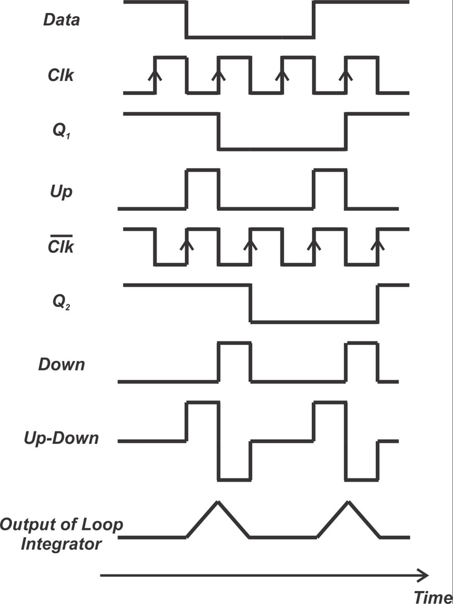
Figure 7. [click to enlarge] The Hogge detector's operation in the locked condition.
As we can see, the Up and Down pulses are generated at separate times. This results in a triangular pulse at the output of the integrator. The pulse increases with a constant slope during the HIGH state of the Up pulse and decreases with the same slope when the Down pulse is HIGH.
This indicates that while the net change in the integrator output is zero, the detector temporarily adds a significant amount of charge to the loop filter and subsequently removes it, causing a ripple in the VCO control voltage. Since a triangular pulse is generated at each data transition, the ripples on the VCO control voltage are data-dependent. This ripple introduces data-dependent jitter into the recovered clock.
In the next section, we'll discuss how a triwave phase detector can greatly reduce this effect.
The Triwave Phase Detector
The output of the loop integrator is usually passed through a lowpass filter prior to being fed into the VCO. A lowpass filter smooths its input signal by attenuating high-frequency components and allowing low-frequency ones to pass through. That smoothing effect resembles averaging.
Consider the average value of the integrator output as a measure of the ripples present on the VCO control voltage. Based on the waveforms shown in Figure 7, each triangular pulse has a net positive area. Consequently, the appearance of each triangular pulse alters the average of the waveform, thereby changing the VCO control voltage.
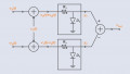
To mitigate this issue, the triwave phase detector substitutes the triangular pulses with pulses that have a zero average. Figure 8 shows the circuit schematic of the triwave detector.

Figure 8. Triwave phase detector.
This phase detector incorporates a third stage composed of a flip-flop and an XOR gate. The second stage output is scaled by a factor of two.
The circuit's waveforms in the locked condition are shown in Figure 9.
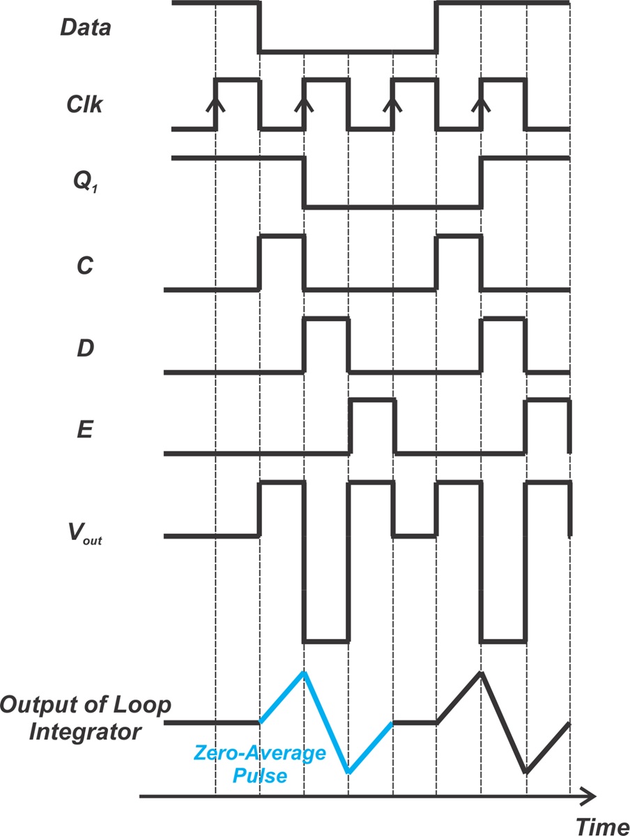
Figure 9. [click to enlarge] Waveforms of the triwave phase detector in the locked condition.
In this case, each data transition produces a ripple pulse consisting of three distinct sections. These ripple pulses exhibit a zero average due to their symmetry around the 0 V axis. As a result, the triwave phase detector significantly mitigates the data-dependent jitter characteristic of the Hogge detector.
Other Limitations of the Hogge Detector
Before we wrap up, it's worth mentioning that the Hogge detector has a few other drawbacks beyond the data-dependent jitter issue. We'll go over them briefly here; for a deeper dive, I recommend Behzad Razavi's "Design of CMOS Phase-Locked Loops From Circuit Level to Architecture Level."
The first drawback is that the delays within practical flip-flops can widen certain pulses, causing a systematic phase offset between the data waveform and the recovered clock signal in the locked condition.
An additional drawback arises from the need for the XOR output nodes, which usually drive a charge pump, to possess wide bandwidth. This ensures the charge pump's current sources can respond swiftly enough to accommodate the target bit rate.
Finally, attenuation through the transmission medium can produce low-amplitude data signals. These may be insufficient to reliably drive the XOR gate at the first stage.
Although these challenges can be mitigated through design adjustments, they may lead engineers to opt for a simpler circuit such as the bang-bang phase detector.
Wrapping Up
In this article, we examined the input-output characteristic of the Hogge detector and highlighted its drawbacks, especially data-dependent jitter. We also introduced the triwave phase detector, which alleviates this issue significantly.
As a final note, although the Hogge detector is predominantly considered within CDR systems, it also finds utility in broader PLL applications due to its resilience against missing input transitions. This sets it apart from many sequential phase detectors, which can encounter issues due to their sensitivity to missing edges. For more on this, see my earlier article "Introduction to the RS Flip-Flop Phase Detector."
All images used courtesy of Steve Arar