Facebook
 Google
 GitHub
 Linkedin
Preventing Runt Pulses in Phase/Frequency Detectors
This article explains the importance of incorporating delay into the feedback path of a phase/frequency detector (PFD) and examines its effect on performance.
The previous article in this series introduced the phase/frequency detector (PFD). This circuit can identify differences in both phase and frequency between its two inputs. It also offers a wide, linear phase detection range.
When designing a PFD, incorporating an appropriate level of delay into the feedback path is crucial. Without a delay, the design's fast feedback loop may cause excessively narrow pulses (runt pulses) at various nodes in the circuit. This is important because other circuits driven by these pulses may malfunction when they are excessively narrow.
In this article, we'll explore how feedback delay can solve the problem of runt pulses. For a more well-rounded picture, we'll also examine the adverse effects of feedback delay on PFD operation. Finally, at the end of the article, we'll wrap up our discussion of the PFD by briefly discussing its equivalent state diagram.
The Problem of Narrow PFD Pulses
Shown in Figure 1 is a common implementation of the PFD. It uses a pair of D-type flip-flops and an AND gate in a feedback configuration to produce the reset signal.
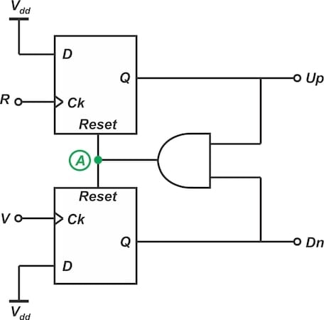
Figure 1. Phase/frequency detector.
Figure 2 shows the typical waveforms of this PFD when the inputs (R and V) are at the same frequency but have a non-zero phase difference.
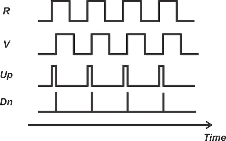
Figure 2. Typical waveforms of the PFD when both inputs are at the same frequency and there is a phase difference.
In this situation, the Dn output produces narrow pulses. This happens because when Dn transitions to a HIGH state, the Up and Dn outputs are both at a logic HIGH, which triggers the AND gate in the reset path.
The Dn output remains HIGH until the flip-flops are reset. The HIGH pulse width of Dn is equal to the total delay of the AND gate plus the reset operation delay of the flip-flops. If the reset path operates too quickly, the pulses may become too narrow for the subsequent stage to function properly. To ensure the PFD operates correctly, it is therefore essential to introduce an appropriate delay in the feedback path.
Above, we had a non-zero phase difference between R and V. Figure 3 shows the typical waveforms when this phase difference is negligible.
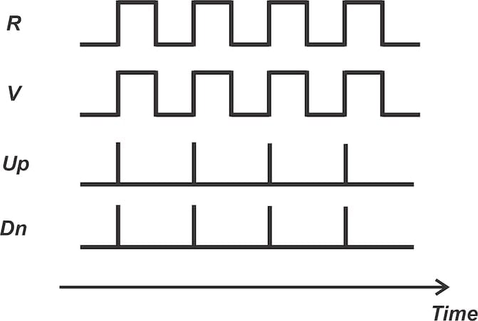
Figure 3. Typical waveforms when the R and V pulses are in phase alignment.
As you can see, we now have runt pulses at both Up and Dn outputs. Since runt pulses can't properly drive the subsequent circuits, we can conclude from these waveforms that a fast feedback path negatively impacts circuit performance near the locking point. Once again, the issue can be resolved by deliberately extending the reset path delay to widen the output pulses.
It's worth mentioning that the short pulses that appear at the Up and Dn outputs near the locking point result in ripples on the VCO control voltage. However, the ripple energy is low, and its spectrum covers a broad bandwidth in comparison to the ripple pulses produced by other phase detectors (the multiplier detector, for example). These properties make ripple suppression significantly easier.
The Effect of Adding Delays in the PFD Feedback Loop
To understand how delays in the PFD feedback path affect the circuit's operation, let's consider the waveforms in Figure 4.
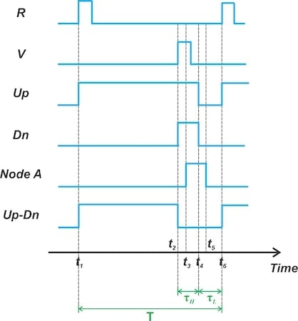
Figure 4. The effect of gate delays on the PFD waveforms.
At time t = t1, a rising edge is detected on the R input. Assuming the flip-flop delay from the R input to the output is negligible, the Up output also rises to a HIGH state at t = t1.
Subsequently, at t = t2, a rising edge appears on the V input. Neglecting the flip-flop delay from the V input to the output, the Dn output transitions to HIGH at t = t2 as well.
At this point, both the Up and Dn outputs are HIGH, triggering the AND gate to produce a reset signal at node A. However, it takes time—the delay of the AND gate—for the reset pulse to reach a HIGH state. Once the reset pulse goes HIGH at t = t3, the flip-flop requires additional time to reset the output, which occurs at t = t4. Hence, the time duration τH shown in the figure is equal to the propagation delay of the AND gate plus that of the flip-flop from the reset input to the output.
The Up-Dn waveform at the bottom of Figure 4 represents the PFD's final output, which is derived by subtracting the Dn output from the Up output. This waveform shows that for a non-zero time duration of τ = τL + τH, the final output is at a LOW state.
A key point here is that once the outputs are reset, they cannot immediately transition to a logic HIGH in response to a rising edge at the inputs. In other words, the value of τL cannot be zero. To understand this, note that when both outputs are reset at t = t4, the AND gate works to bring the reset signal at node A down to a logic LOW. Due to the delay of the AND gate, this can't happen immediately.
Additionally, once the reset pulse goes LOW at t = t5, the flip-flop needs some extra time to recover from the reset before it is ready to detect upcoming rising edges at the inputs. The minimum value of τL is therefore equal to the propagation delay of the AND gate plus the recovery time of the flip-flop from a reset.
Adverse Effects of Feedback Delay on PFD Performance
As mentioned above, the Up-Dn waveform in Figure 4 represents the final output (Vout) of the PFD. Let τmin represent the minimum value of τ, and let T denote the period of the input signal (see Figure 4). In this case, the average of the Up-Dn signal has a maximum of:
$$\overline{V_{out}} ~=~ \frac{V_{dd} ~\times~ (T~-~ \tau_{min}) ~+~ 0 ~\times~ \tau_{min}}{T} ~=~ V_{dd} ~\times~ (1- \frac{\tau_{min}}{T})$$
Equation 1.
From the previous article, we know that the gain of the PFD is:
$$k_d ~=~ \frac{V_{dd}}{2\pi}$$
Equation 2.
Dividing the average value from Equation 1 by the PFD gain, we obtain the maximum phase error that the PFD can detect:
$$\Delta \phi_{max} ~=~ \frac{\overline{V_{out}}}{k_d} ~=~ 2 \pi \times (1~-~ \frac{\tau_{min}}{T}) ~=~ 2 \pi ~-~\omega_R ~\times~ \tau_{min}$$
Equation 3.
where ωR is the angular frequency of the input.
The ideal PFD we examined in the previous article had an input-output characteristic with a linear range of –2π to +2π. Because of the non-zero gate delays, a practical PFD can't achieve this. Instead, Equation 3 shows that the maximum detectable phase error depends on ωR and τmin.
Example: Determining the Linear Range of a PFD With Non-Zero Gate Delays
Consider a PFD utilizing a flip-flop with the following parameters:
- A reset operation delay of 2.5 ns.
- A reset recovery time of 3 ns.
- An AND gate delay of 1.5 ns.
Given an input signal frequency of 25 MHz, what is the maximum phase error that the PFD can detect?
Solution
To answer this question, we first determine the time durations τH and τL. The duration τH is equal to the propagation delay of the AND gate plus the flip-flops' reset operation delay, resulting in τH = 1.5 + 2.5 = 4 ns. The minimum value of τL is equal to the propagation delay of the AND gate plus the flip-flops' recovery time, producing τL = 1.5 + 3 = 4.5 ns.
Therefore, the minimum interval that Up-Dn is LOW due to the non-zero gate delays is τmin = τH + τL = 4 + 4.5 = 8.5 ns. Substituting ωR = 2π × 25 MHz and τmin = 8.5 ns into Equation 3, the maximum detectable phase error works out to:
$$\Delta \phi_{max} ~=~ 2 \pi ~-~2 \pi ~\times~ 25 ~\times~ 10^6 ~\times~ 8.5 ~\times~ 10^{-9} ~\approx~ 0.79 ~\times~ 2 \pi \ \text{radians}$$
Equation 4.
Thus, although the ideal PFD can detect a maximum phase error of 2π radians, the specified gate delays decrease the maximum detectable phase error to 4.95 radians—a reduction by a factor of 0.79.
Equivalent State Diagram of the PFD
Earlier in this article series, we learned that the RS flip-flop phase detector can be modeled as a two-state device. Its state diagram is illustrated in Figure 5.
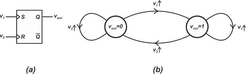
Figure 5. The RS flip-flop phase detector (a) and its equivalent state machine (b).
The PFD can likewise be modeled by a state machine. A cursory analysis shows that the PFD is equivalent to a state machine with at least three distinct states:
- State 0: Up = 0, Dn = 0.
- State 1: Up = 1, Dn = 0.
- State 2: Up = 0, Dn = 1.
This is illustrated in Figure 6.
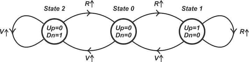
Figure 6. The state diagram of the PFD circuit.
When the PFD is in state 0 (Up = 0, Dn = 0), a rising edge on input R transitions the system to state 1 (Up = 1, Dn = 0). The circuit stays in this state until a rising edge on input V resets the flip-flops, returning the system to state 0.
As Figure 6 illustrates, a rising edge on input V causes the system to shift from state 0 to state 2 (Up = 0, Dn = 1). The circuit remains in this state until a rising edge on input R resets the flip-flops, bringing the system back to state 0 (Up = 0 and Dn = 0).
It's important to recognize that the state diagram above is only a basic model of the system. As illustrated in Figure 4, both the Up and Dn outputs can briefly be HIGH at the same time. Consequently, a more precise representation of the system would incorporate a fourth state where Up = 1 and Dn = 1.
Wrapping Up
A primary consideration in PFD design is to prevent the formation of overly narrow pulses at various circuit nodes. These runt pulses, which may arise due to the fast feedback loop utilized in the design, can lead to improper functioning of subsequent stages. To guarantee proper operation, it is therefore vital that we implement a suitable delay in the feedback path. However, it should be noted that the feedback delay restricts the maximum detectable phase error as well as the maximum frequency of operation.
All images used courtesy of Steve Arar